[Request] ASUS PRIME Z490M-PLUS BIOS with 11th Gen CPU Support

Asus Q470, no support for 11th generation either, that’s in it’s way OK. But this is a ‘enterprise’ chipset, board has afaik extended warranty, too, but no bios updates since 2021, neither ME updates.

Mailed them, uninterested answer.

Asus had kinda bonus for many outstanding products, still remembering the P55T2P4, but you can’t expect good support any longer.
Regarding their products: Don’t expect anything more than what’s really in the box!

1 Like

I agree with you.
But this community could change that.
Imagine the shock for their customers: some people make their own bios and demonstrate that some product are not upgraded for profit!
What a shame!

Ok! now it’s time to work.
No support from asus, we’re alone on this problem.
i’ve booted my mainboard, with a 10th gen proc, to seek some info.
it’s the last bios from asus: 1621 of 2021/11/19
the ME version is 14.0.33.1125.
There is the possibility to upgrade the ME version to 14.0.45.1389 V2.1
The bios is a .cap.
but i’m still lacking a lot of info/understanding of how these bios are working/made.
I understant there is a proc part where we declare different type of procs (cpu mcodes)
In my case, there is only 10th gen procs in ?
But what is exactly the role of the ME? is there a relation between the cpu mcodes and the ME FW ?

A big thank @MeatWar for his precedent post! very good informations! Obviously, i’m a bit slow compared to him :wink:
What is SPI IC(s)? are they the different part of the bios?
There are tools for 7,8 and 9 series chipset asus. Is 490 a 4 serie? incompatible with those tools?
What should be my first test to explore these tools and make my choice on the best tool for my case?
Where could y download those different parts (cpu mcodes and ME) i should insert in my future modded bios?

Still a long road to follow.

Even with an Updated ME, there would still no menu for Rocket Lake specific bios settings like gear 1 and 2 for memory, rocket lake specific voltage settings, and others. The best thing you could do is to crossflash another board bios, like Prime Z490-A for example.

If you do want to flash a Z490M-Plus “Frankensteined” ME 14.1, you could try this (i use PPHY Region and SAMF Region from TUF Z490 Plus), i also include the ME.bin for fwupd use only if you ever want to try update the ME region only (ME 14.1 with latest pmc, pchc, and phy p cmp): PZ490MP.rar (8.2 MB), please note to DWYOR since i wont gurantee this bios would be able to run Rocket Lake, let alone boot Comet Lake. Better back up your current bios with ch341a or any programmer before doing so.

@Kokieezz
Thank you for your advice.
You’r right, the TUF Z490 Plus is the asus mainboard most alike the Prime Z490-M Plus on the component level. And this one had the right to have an upgraded bios to 11th gen.
So i’ll try to write the bios of this one on my mainboard.
Too bad, no security for me: the bios chip is soldered and not compatible with those a ch341a could backup. It’ll be a win or lose attempt.

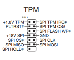
Actually, you might able to. Either use a soic8 clip, OR use the TPM header using dupont arduino cables with 2mm pitch to connect directly to ch341a, you could learn the same logic here: [Guide] ASrock SPI_TPM_J1 Pinout for CH341A and other programmer + Flashing it , measure +18V SPI if it is 1.8v or 18v, and check your bios chip part number online to see if your bios chip is within the operating range of 1.8v or 3.3v before doing so.

Here is your Pinout based on your motherboard manual (only those that labeled as “SPI” that are need to be connected to ch314a programmer):
image

I do really suggest to back it up first, because either success or not, if the z490 wont be used it could be sold.

@Koekieezz
Many thanks for the reply.
So, in fact, the boardmakers have added a connector permitting the direct access to the EEPROM chip of the bios? that’s it?
There is 2 parts on this connector, does that mean there are 2 different chips accessed by this connector? bios chip and TPM chip?.
Of course, if the backup and/or rewriting of the bios can be done, with the mainboard off => without any access layer control from the board, does that mean you can have full control or is there any locks remaining? maybe some unknown certificates to encode the bios => obligation to use some bios of the mainboard maker.
And for the TPM part, could this give access to the crypto part of the TPM? (that would be a major breach in the security, but i would’nt complain about it)
If that can rewrite a bios, why waiting? why not rewriting it now, and use the downloadable, official bios if that goes wrong? Unless the bios is crypted and we need an unencrypted one to write it… the .CAP <> the.ROM ? And with the .CAP and the correspondent .ROM , we should be able to obtain the certificate used to encrypt it?
Do you know if assus change the certificate for each model? for each rom version? for each mainboard?
OK, more and more questions, sorry about that, i’m currious.
I"ll follow the steps you kindly gave me, i’ll bought a ch314a programmer and proceed as you described.
Next step: receiving the ch314a and using it to backup the bios! :slight_smile:

By looking more closely to the card, i’ve identified (i think) the bios chip
MX25l12872f.
So many chips on those mainboards…
But it was logically close to the TPM connector.

I wont be answering your question regarding why TPM header have SPI pins since i dont really know why and how dedicated physical tpm works, i would suggest probably it is required for some “handshake” between the bios and the ftpm.

The .CAP is only a capsule (as for now) and you could delete the first 0x9FF region of the bios to obtain the actual bios, or the so you call .ROM ones (with the capsule header removed it will be 2KB less, which rounds perfectly with the size unit).

For certificate changes and such question, probably sweet kitten might know, or other gurus might know abt it.

Every answer and thoughts i have here are learnt mostly rom here and other forums, so you might want to start answer your curiosity by searching any kind of problems and unsolved problems, the world of bios modding is vast, who knows you could find a way to “Mimic asus .cap signature” or such, since it would be a great news for bios modder.

Well, i finally received my CH341 programmer.
As i said previously, i’m slow compared to experienced users of this board :wink:
I still have much to learn before being at ease, so i will make my first attempts on another Board: an old assu (again! odd!) H61M-K.
This board is simpler, i can remove the flash chip.
After reading the reference of the chip, it’s a 3.3v, so i had to verify my ch341 programmer was in 3.3v…it was the case, so i went straight to the point of reading the bios chip!
The harder has been to stop the driver signature with the small laptop i’m using for the process (win 7 pro). But i succeeded. I downloaded the asus bios (.cap, i will have to convert in .rom before trying to write it back in the chip).
Back to the Prime Z490M, i feared i would have to by a voltage converter (because of the 18v SPI mention, i feared the bios chip was in 1.8v). Th chip is a 25l12872f, and it’s operating in the 3.3v => i won’t have to have a converter then.
If my experiences with the old H61M-K are OK, i’ll try the reading of the Z490M with the soic8 clip…
Whatever what will happen, a great thank @MeatWar @Koekieezz @Fernando and @lfb6
I’ll continue reporting of the progress.

Ok, the test on the H61M-K chip has been made.
I was able to read the chip, transform the .cap file in .rom, and reflash the chip.
Unfortunately, the MB was already KO, so i didn’t had the chance to see the results.
Now, for the Z490M-Plus, i have a trouble… the chip can’t be detected.
I suppose it’s because the MXIC MX25L12872F
isn’t in the database of the ch341 programmer V1.29 ?
I’ll have to make others attempts to be able to read the chip.
A long road indeed :wink:

Try to take off the z490 board cmos, and use neoprogrammer 2.2.10 instead

Ah, but the chip is soldered on the MB… i’m trying with the clip.
But i agree that add a lot of variables to the equation… i don’t know if the electronic circuitry on the MB could change the communication, or even if my clip is functioning. I’ll have to make other tests to validate the clip, then other software’s to communicate with this chip.
Thank you all for the great support you give, better than a course! it’s the best practical work I’ve ever made :wink:

Instead of using the clip, you could try to use the asus SPI_TPM pins using dupont/arduino jumper cables like what i mentioned on post #14

Well, i think you’re right, that would lesser the clip8 variables.
However, there are some difficulties for me to connect to the SPI_TPM pins.
I don’t know the right voltage on it (i’ll have to make the measurement), i don’t have a device for plugging to the pins, and i don’t have a software to recognize the chip…
I’ve found a dell optiplex 3020. The chip is soldered on the MB (as the asus) and is a MX25L6473E.
I’ve downloaded different version of the ch341progammer, and the last one has this chip in his database. Unfortunately, my tests with the clip was a failure… unable to recognize/discuss with the chip. Ans the asus chip isn’t in the database either :weary:
I should make some conduct tests on my clip maybe, read notices again… nobody heard of locking systems on the bios chip? perhaps i should test them with the MB powered on (don’t like the idea)…
Still many paths to explore…

No and feeding more power to the circuit is always the LAST resource and NOT common on desktop mboards.
NeoProgrammer 2.2.0.10 has the MX25L12872F on his db.

Yes, i feared that would be a risky way. I won’t do it without good reasons or mastering of the process. :slight_smile:
Apparently, the clip have very low chance to work when the chip is soldered on the MB.
That mean, the best way is to use the SPI_TPM pins…as mentionned by @Koekieezz :+1:
I need to by dupont jumper cables before having a try.
Thank you again for your support.

Yes, in this model the SATA ports are an obstacle. Users with soldering/desoldering experience will take it out to program.
Other will even solder direct conductor cables to each pin of the IC
There is “other kind” clips of the web from our ingenious CN citizens and their web market… not cheap not common not easy to find in some parts of the globe etc…

Well if the IC model is the one referenced before (MXIC MX25L12872F) by you… then its not 1.8V, its 3,3v.

:+1:
I need some time to make the experimentation. We’ll see if that works, and if the 18v is indeed a 18v

Well, i finally sacrificed a old acer veriton l460 of my collection, to have a correct cable.
I was looking for the pin correspondances, when some details makes me wonder…
On the asus connector, there are the connections, i should use SPIxxxx
image
But there are 10 pins with the GND…
I suppose i don’t have to count the SPI TPM then…
SPI HOLD, SPI MISO, SPI CS, SPI MOSI, SPI CLK SPI FLASH WP,+18v SPI and GND would be the pitch.
But, looking at the MX25L12872F, there are those pitch reported: CS, SIO0,SIO1,SCLK,SIO2,SIO3,VCC and GND
Looking at the map, i see why the clip didn’t work… the pin assignment is different (the N°1 is not the vcc), so i should have to rearange that for the clip to have a chance to work…
Now, let’s figure out who’s who on the pin side.
GND,VCC,CLK,CS are easy to guess.
But MISO,HOLD,MOSI and FLASH WP vs SIO0,SIO1,SIO2,SIO3 ?

Maybe i should look into ch341a notice to try to understand the right correspondence?