Lenovo D30 Thinkstation C602 chipset ME7 Sandy Bridge to ME8 Ivy Bridge support

There are two Lenovo D30 Thinkstation machine types (MT):

MT4223,4228,4229
A1JxxxUSA bios/uefi
Intel Active Management Technology 7 (SB)
Security chip: Nuvoton NPCT421L for TPM function
Realtek®ALC662 codec
Two LGA2011 sockets, supports up to two processors from Intel Xeon E5-2600
Dual onboard gigabit ethernet, Intel 82579 and 82574
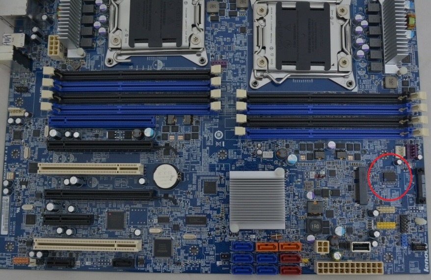
Motherboard: Descartes rev 1.0, Descartes rev 1.1

MT4353,4354
A3JxxxUSA bios/uefi
Intel Active Management Technology 8 (SB/IVB)
Security chip: STMicroelectronics ST33TPM12LPC for TPM function
Realtek®ALC662 codec
USB 3.0 capability – with tracings and hardware added to the main board
Two LGA2011 sockets, supports up to two processors from Intel Xeon E5-2600 v2
Dual onboard gigabit ethernet, Intel 82579 and 82574
Motherboard: Descartes rev. 2.0

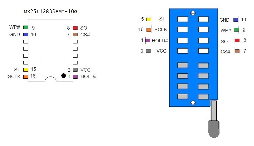
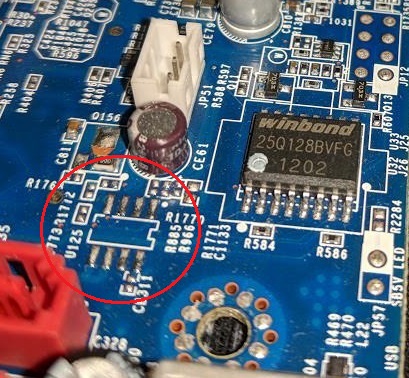
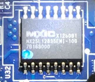
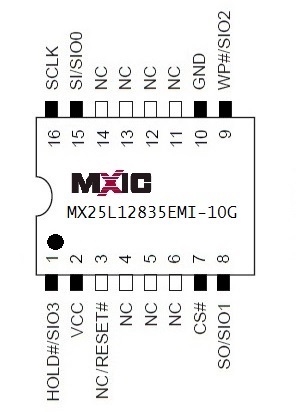
SPI chip - MX25L12835EMI
The D30 motherboard uses a 16MB, 16-pin SOIC chip by Macronix International Co., Ltd.

D-30 SPI location.JPG

MX25L12835EMI.jpg

16-pin SOP MX25L.jpg

[[File:SOIC16_rw(1).jpg|none|auto]]
Although there are 16-pins, only 8 pins are actually involved in communication and these are the ones that are used to program the flash memory using the CH341A Programmer and a SOP16 clip. I will be using ASProgrammer 1.41 as it has the SPI entry that is required in their drop down list.

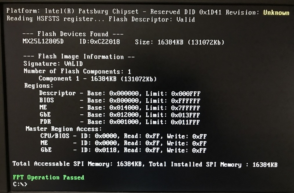
hardware dump method
The bios chip has 3.28V of power between pins 2 (Vcc) and 10 (GND) even when the computer is turned off, but power cord still plugged in. I’m not sure why? Still, I removed the power cord completely. My attempts to read the SPI chip failed. I was obtaining “FF” with the chip_ID selection using the CH341A_SPI programmer. I don’t think it has enough power as this is a very large motherboard with dual CPUs and lots of memory slots. Plugging the power cord back in and retesting didn’t work. Powering up the computer to a POST and attempting the dump also didn’t work, probably because it was interfering with the data lines when active. I unplugged everything again. I purchased a variable external DC power supply similar to what @gyrator used. I turned up the amperage to 600mA and voltage “fine tuned” it very slowly upwards until I got to around ~3.4volts. ASProgrammer was finally able to recognize the chip and dumped the entire SPI contents. The SPI dump had UEFI errors when parsing it using UEFITools. ASprogrammer didn’t work for me. I used CH341A Programmer Version 1.18, this finally got me a very accurate SPI dump without any parsing errors.

software dump method
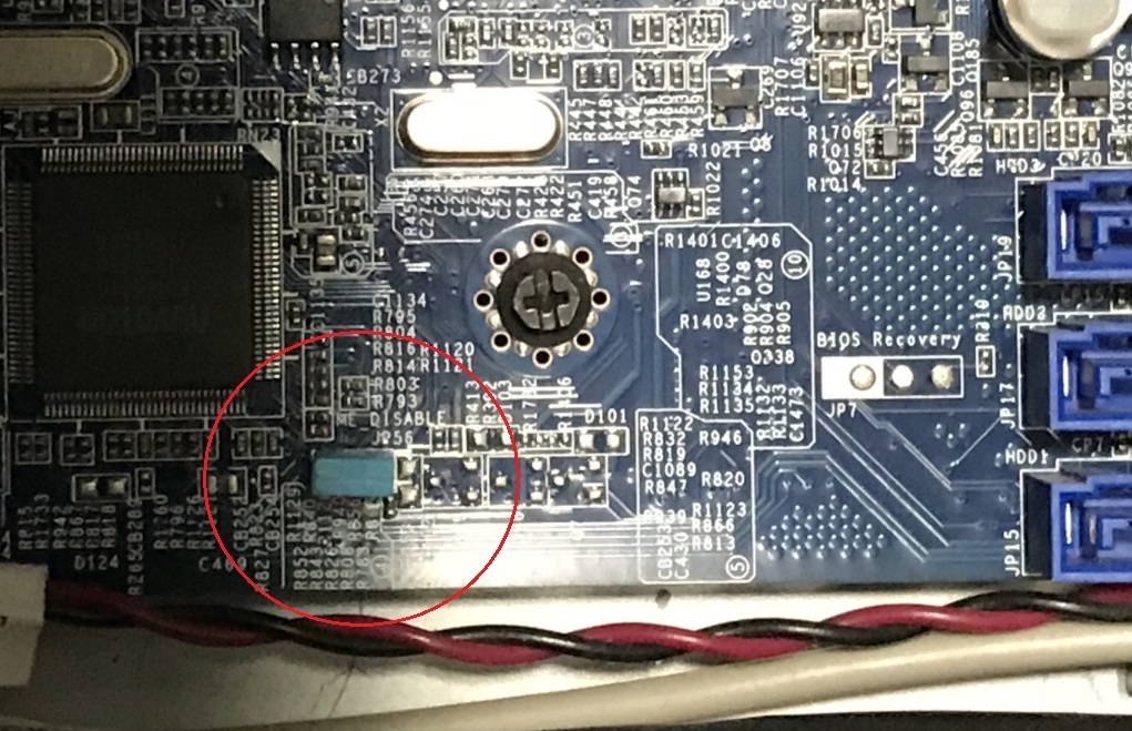
A full software SPI dump can be achieved by jumping pin JP56, it is labelled: ME_DISABLE

ME_DISABLE JUMPER56.jpg


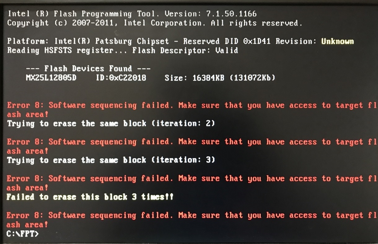
This will allow a dump of the full SPI image using fpt -d spi.bin. I’ve already applied the “FF” bytes to the 3 main areas of the descriptor code. No need to use any pin-mod here.
Once I altered the descriptor region and flashed it back into the bios, I didn’t need to use the jumper any longer for future flashes. However, the BIOS region has 2 major protections, FLOCKDN bit and BIOS_CNTL. These need to be overcome to get fpt to fully work.


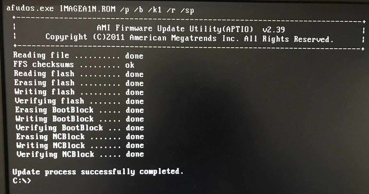
Thankfully, the OEM manufacturer, Lenovo has created an ivb-capable bios A3J366USA. They only made it possible to use in the MT4353 and MT4354 machines because these have been outfitted with ME8 firmware (hopefully that’s the only restriction).
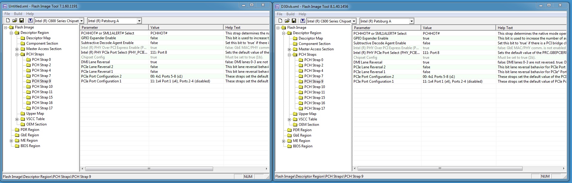
I opened FITc v7, loaded the original SPI dumped image and kept the window open.
Opened FITc v8, adjusted the SKU at the top (C600, Patsburg A), then imported the: BIOS Region (A3J366USA bios), GbE Region, OEM, PDR from the FITC v7 decomp folder.
Next, I imported the ‘8.1.72.3002_5MB_PRD_RGN’ at the ME region and afterwards manually adjust every single FITc v8 setting found at the tool to match the values from FITc v7 ME region.

Problems
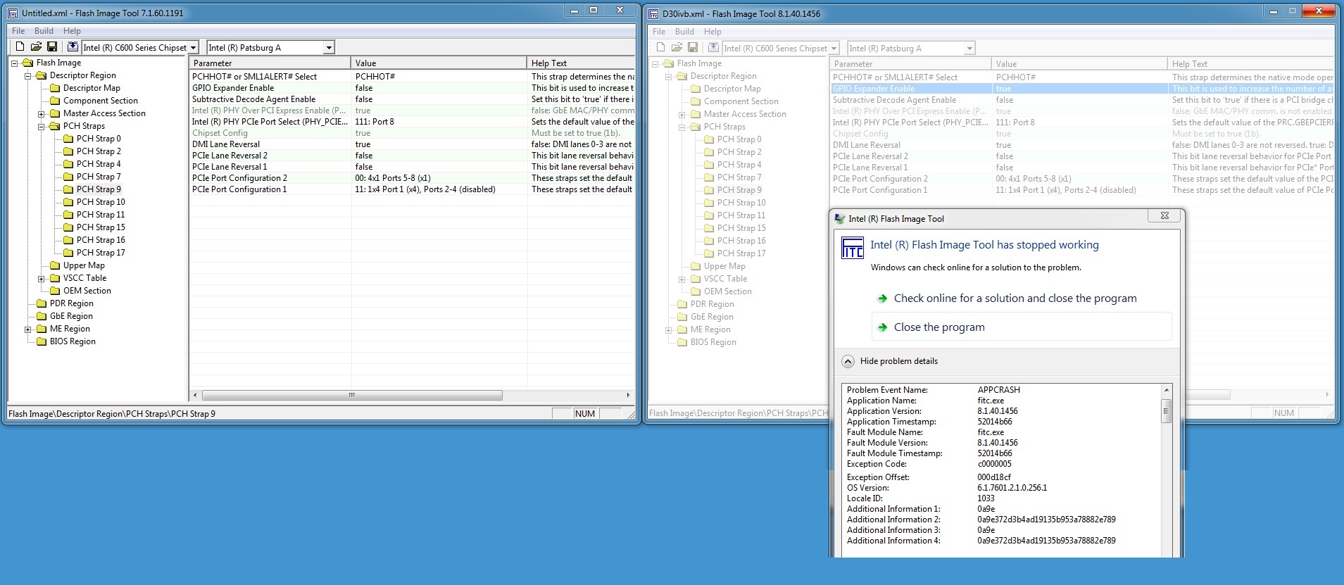
There is a FITc v8 crash when I adjust the GPIO Expander Enable parameter from ‘true’ to ‘false’

GPIO error.jpg

GPIO error2.jpg


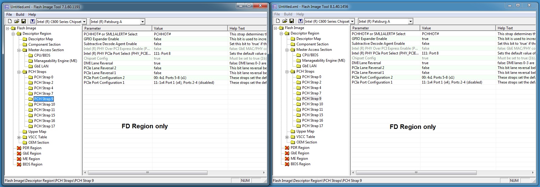
When I load the File Descriptor region only in both versions of the software I get this:

FD region only.jpg


So I plan to just leave this alone, and see what happens.

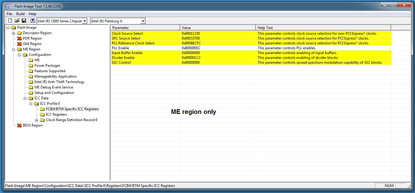
When I open up the ME7.1 region by itself in FITc v7 (SKU: C600, Patsburg A), I get these values:

me region only.jpg


When I load the full SPI image in FITc v7 (SKU: C600, Patsburg A), and look at the ME tab, I get these values:

full spi image.jpg


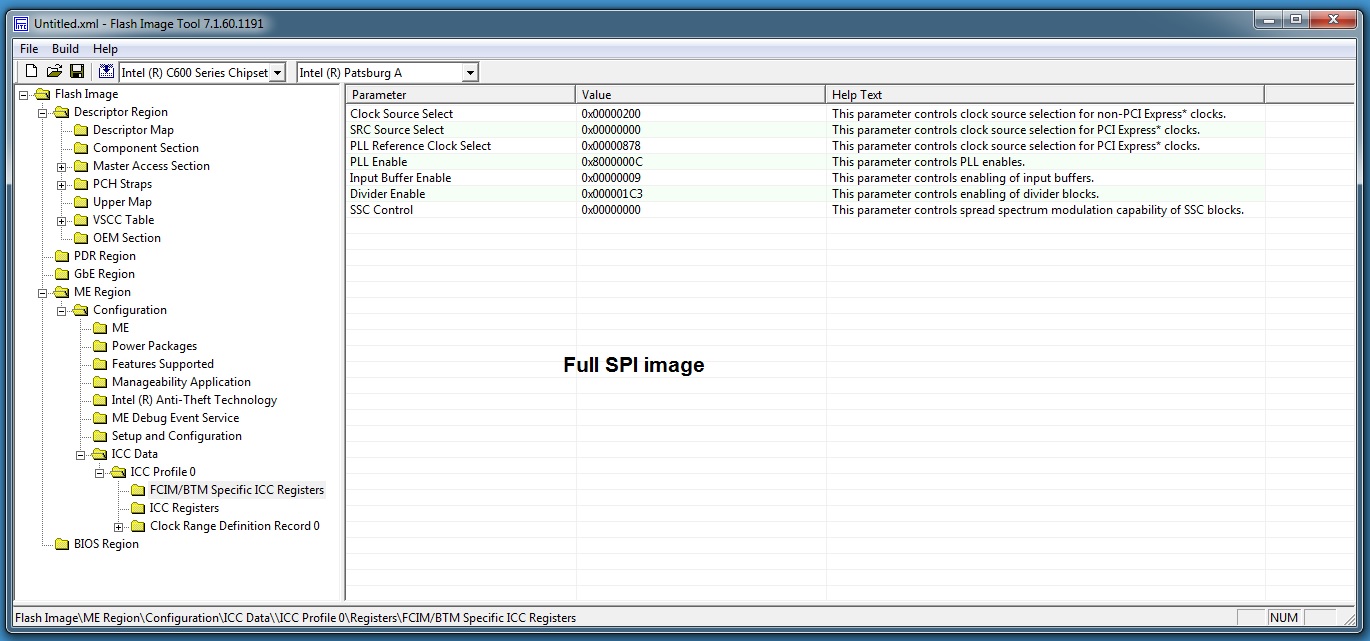
I believe these values in the above pic are known as default values, because when I change the File Descriptor:PCH Strap 17 to “buffered through mode” a window pops up that says all the ‘FCIM/BTM Specific ICC Registers’ will be reset to default.
The original SPI image had PCH strap 17 set to “buffered through mode” so I’m thinking it should be that way, but why are the ME Region values by itself so different?
per @plutomaniac , it likely is the FITc bug reported in other posts here.

My solution to this was to drag/drop the desc.bin region right into FITc 8 right from the beginning and then use a separate instance of FITc 7 that has just the ME Region loaded it, and then edit the FITc 8 ME region accordingly, they then matched up without conflict. I loaded in the other regions (GBe, PDR) per usual with the input-file command. So basically, the only editing to do is in the ME tab.

SOIC16_rw(1).jpg

Very nice posting.
I have a similar case here. Actually the S30 board, which is very similar, despite being only a single socket version.
And it’s also the version that is for E5-2600v1 only. However, I would really like to use it with a E5-1650v2, that I have.

As the procedure itself should be pretty much identical on my board, I will closely follow your progress. THANKS!

desc.bin has been altered to include bytes "FF" for main region access

AFTER FF.JPG


in a Freedos window when I execute:

1
 
 fpt –BIOS –f IMAGEA1N.BIN
 
this causes this Error 8: software sequencing failed

Error 8.JPG


However when I use AFUdos, the BIOS file is written correctly and is functional.

1
 
AFUDOS.exe /IMAGEA1N.bin /p /b /k1 /r /sp 
 

AFUDOS FLASHES OK.JPG


What is an error 8, and what is the ‘magic’ that Afudos is doing that FPT can’t.

addendum: I found a little discussion from CodeRush years ago on this issue:
“FPT is in fact more reliable then AFU, because it’s much simpler and does no changes to input file, while AFU tries to preserve ROM holes, transfer some files and do other things no one really needs. Then it uses SMM-based flasher to do real writes to SPI chip, which can be handy on boards with BIOS Lock, but again more complex then FPT, that just uses chipset registers directly to write to SPI chip. You don’t have to worry about FPT or AFU. If writing with FPT works for you - go use it, if not - just use AFU, either way is fine.”

BTW, maybe the following hint could turn out to be helpful:
On the S30 there were standard SOIC8 pads below the SOIC16 flash.
I replaced the original SOIC16 flash with an SOIC8 part that was supported (fitc will tell you which ones are).

And with that it is much easier to use external programmers and for example a standard SOIC8 clamp.
I would venture a guess, that it’s the same layout, concerning the SPI flash, on the D30, too.

@celemine1gig , interesting idea. I have both SOIC16 and SOIC8 clamps so I think I’ll be okay.

I’ve looked at the VSCC table for the D30 & S30, they both show the exact options:

Flash chips in VSCC table:
1F4700 (Atmel AT25DF321)
EF4017 (Winbond W25Q64)
EF4018 (Winbond W25Q128)
C22018 (Macronix MX25L128)

Your board is interesting in that it has that option, I never knew you could do that. Good job!

S30 dual bios.jpg


which chip did you choose?

@celemine1gig - good tip! Here’s mine on the same level, you can edit whatever chips are compatible too, by editing the VCSS table in ME FW with Intel FITc tool, so you can add chip ID if you need and it’s not there.

@nikey22 :
If I understood it correctly, this worked perfectly fine for your D30, right?

Tried the same thing for my S30 today and I only get until the very early POST-Code 04 and then it stops.
Will have to look further into it. Maybe I missed a setting.

Besides that, I saw the exactly same issues while trying to port the settings from ME7 to ME8, like described by you.

@celemine1gig
no, this has not worked yet for me!

I’m still trying to figure out why. I tried to hardware flash the SPI image with the ME8-A3 bios combo, but as you said, it doesn’t proceed past the post-code, I don’t remember which one it was for me. One time, I was able to get the “Lenovo” name on the screen, but it froze after that. Then I got some memory code beeps.

I will try the software way, fpt each section this time, the ME region and the BIOS region.
I was able to software flash the ME8 region, it did a normal post beep, but it didn’t talk well with the A1 BIOS, there was some kind of kernal panic message at the top of the screen, but I was able to ‘F1’ into the CMOS settings, then I turned off ME subsystem, got back to the DOS prompt and re-flashed the ME7 region back in, and rebooted to recover from it.
I think the problem might be in the A3bios. We’ll have to look into it further

It would help if someone who had a IVB machine type could send us their SPI-image to investigate it further!


Agreed.
I have no idea if it would give us an idea right-away, but anyway, would be nice for comparison purposes.

@celemine1gig , try to flash your original bios back into your chip, just to see if it is possible. Can you do that?

fpt -bios -f bios.bin

Tell me if you are getting a "software sequencing failed…" error.

I won’t get that, as I cannot boot anymore at all.
And besides that, I have a hadware programmer. Never used any other method on that board.

Programming back the old bios will be no problem at all.

@nikey22 @Lost_N_BIOS I am trying to flash the BIOS ROM chip on my D30 motherboard as well. I have the CH341A programmer with the SOIC8 clamp but this chip is an SOIC16 chip. According to the above it only uses the 8 pins starting from pin 1 for communication though, does this mean I can still use the SOIC8 clamp to read/flash this chip or will I need an SOIC16 clamp? When I get a good connection to the chip the CH341A software reads $00 for everything and can’t detect the chip…however if it doesn’t connect to those 8 pins it only reads $FF so it seems to be seeing something. Not sure if it needs the other 8 pins to actually detect the chip or not. Thanks

Help is needed from experts.
Hi, my pc Lenovo s30 (machine type: 435, model: D32,… motherboard: Socrates rev 2.0) bios have been corrupted during windows 10 pro updating, I was using windows 8 and I manually installed a fresh windows 10pro-64bit, after installation finished i checked for updates in the setting -windows and updates, it was going good for 40-50 minutes untill when windows were updating its components and then a message windows pop up saying shuting down, after shuting down it starts and fan spins and after few seconds its get off and restart again for few seconds and its stuck on this loop forever, i tried, to reset bios by cmos battery removal, and cleared cmos using jumper as per the manual, tried also a bios recovery but no luck, at last, i have ch341 programmer laying around so i tried to read the old bios(dumps) , its a 16ping flash rom named as: MX25L12835FM1-106, So igoogled and find some one on this forum has read the chip so i follwed the steps and able to read the dumps, but i am not programers nor computer guy and dont know how to repair my bios if possible or replace with new bin file which i dont know to extract from bios,
so help is needed if someone can have a look at my bios dump and can fix it, or extract me a bin file that i can write to the chip,
note: This motherboard has no error code display screen like some have, and there is no beep, just a starts-off-restart with no display on screen complete blank no input
Thanks
.
here is the link for old dumps, and images of the system model
https://drive.google.com/drive/folders/1MKI3T6fZEmBkla1VqZNFoOb0q1cUNmze?usp=share_link