i contacted asrock support and they confirmed that the layout matches the one mentioned in the asrock J3455M manual. according to that layout the solution for spi25 chips would be as follows:
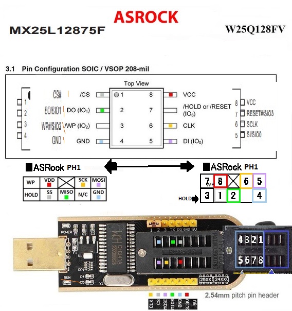
i copied all the info needed from various sources into one picture to make it as easy and understandable as possible ( yes im no graphics designer  ) hope that helps couple of you out there, cause even i suspected that the layouts are the same, we only got 1 try maybe and i don’t wanna start soldering a new chip
greets