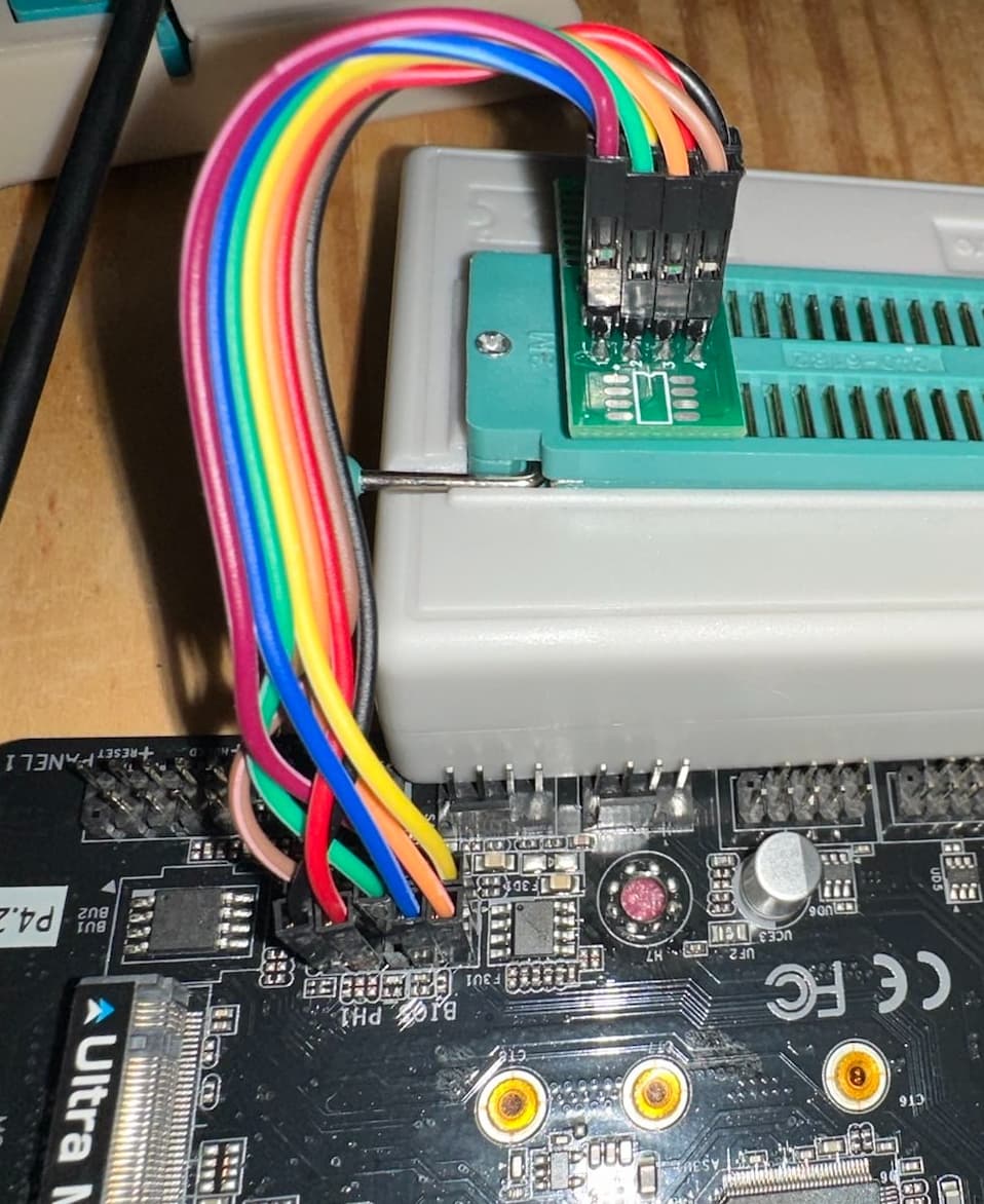
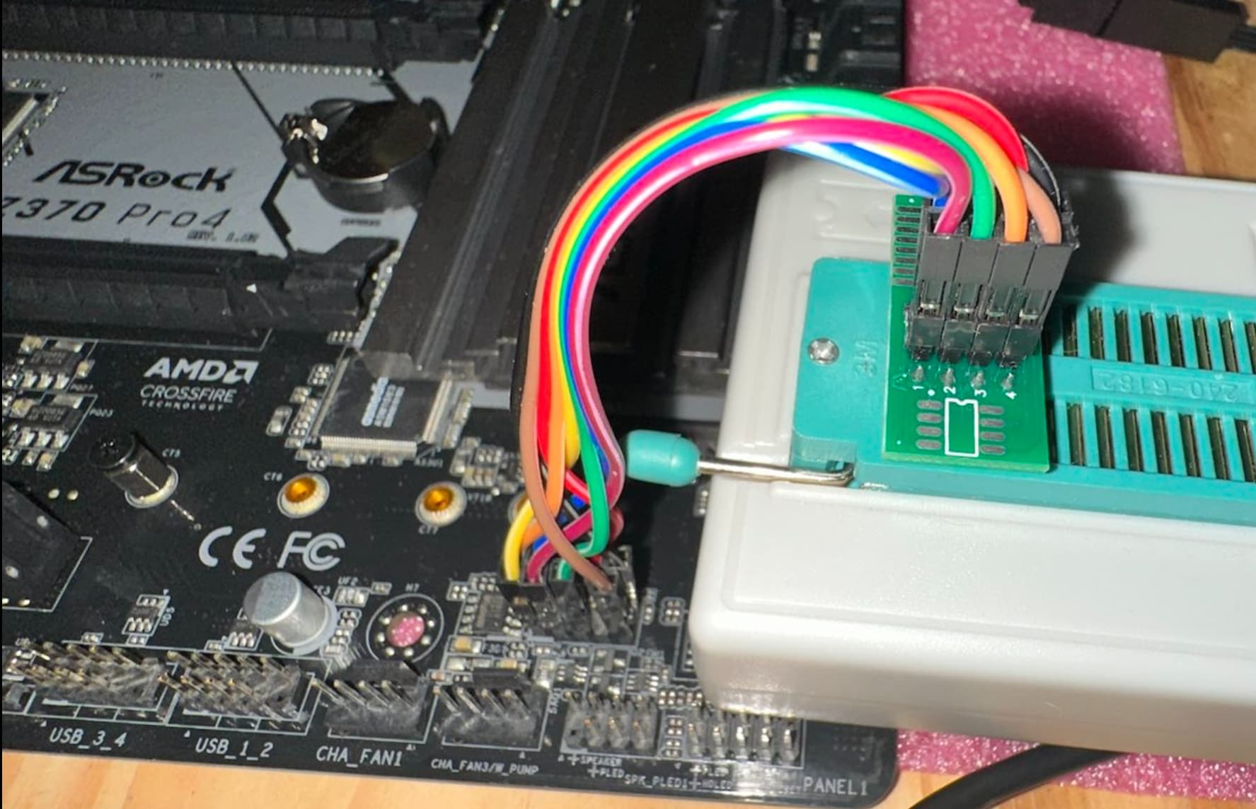
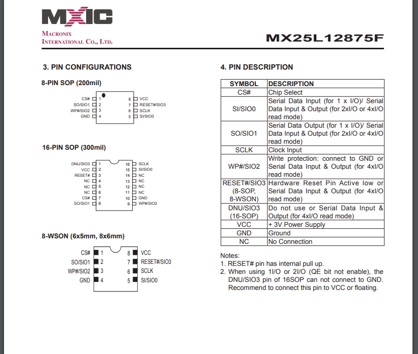
i bought a CH341 A, unfortunately the clip doesnt fit well on the chio and its not removable so i wanna try it through the bios_ph1 header, i just dont know which cable to buy and appreciate your help. i will add any info which could be useful for finding it out below.
found this from another forum regarding to a "ASRock Z370 Extreme4 "
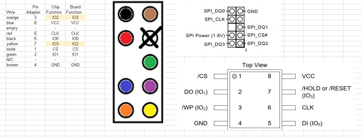
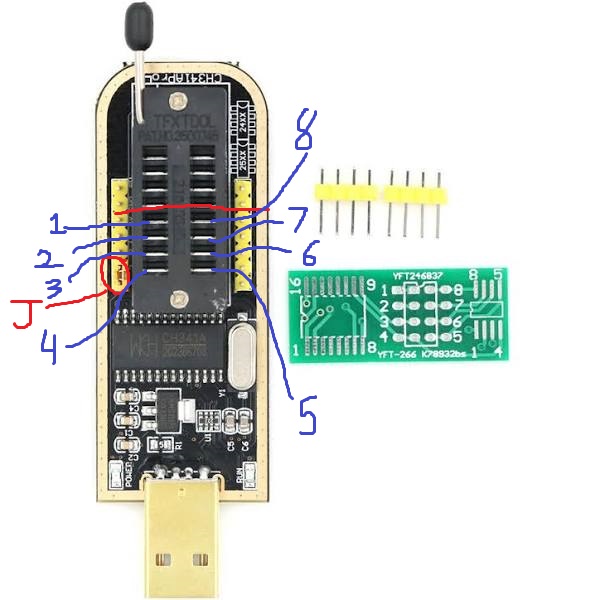
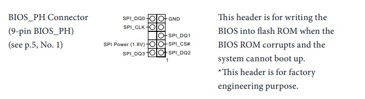
probably there is not a one click buy solution maybe …if i decide to make a custom cable with jumper wires(male to female)…could you please help me where i would have to connect each cable on the PH1 header…i only know the layout of the ch341 which is this:
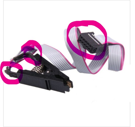
or would it be possible to remove the 8 cables from the spi slip and use those instead? where would i connect them in the ch341? pin1 is also marked in red on my cables (my cable is 8pin)
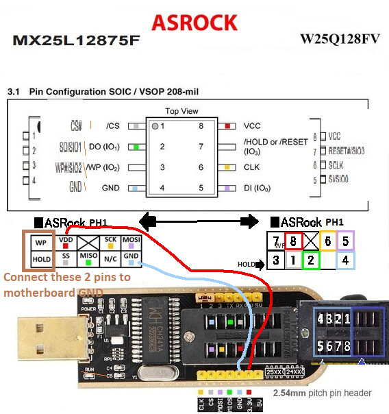
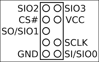
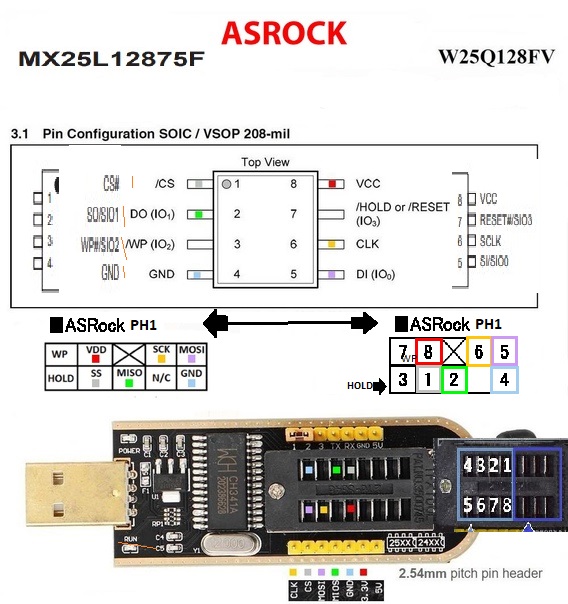
i contacted asrock support and they confirmed that the layout matches the one mentioned in the asrock J3455M manual. according to that layout the solution for spi25 chips would be as follows:
i copied all the info needed from various sources into one picture to make it as easy and understandable as possible ( yes im no graphics designer ) hope that helps couple of you out there, cause even i suspected that the layouts are the same, we only got 1 try maybe and i don’t wanna start soldering a new chip
Thanks, it helped me a lot, you really need to ground the 2 leftover pins, first I flashed the bios, then I shorted the bios mode selection and flashed again (so both bios are updated)
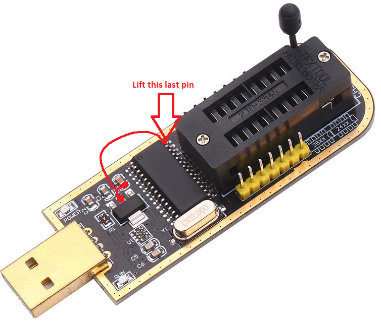
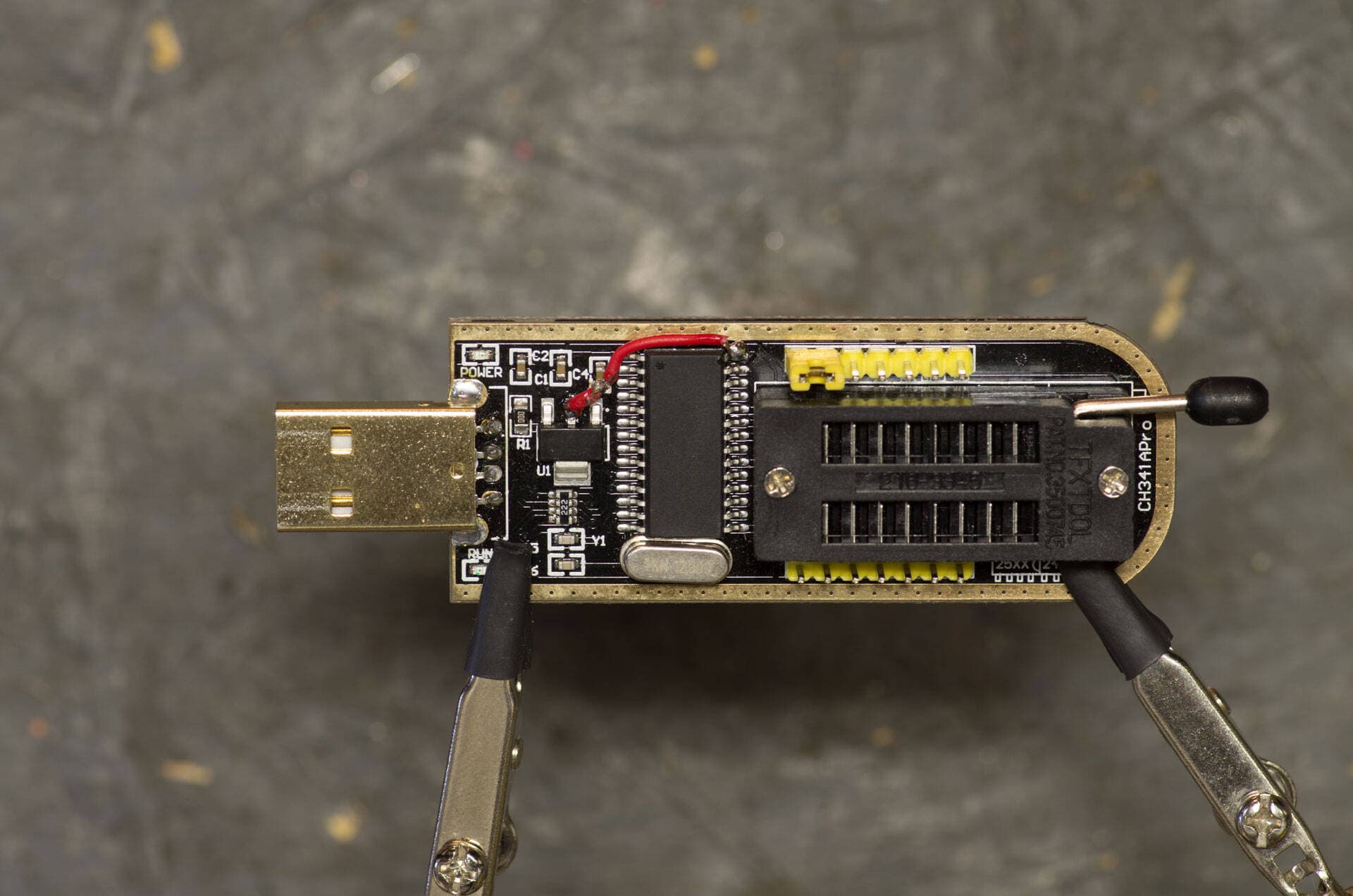
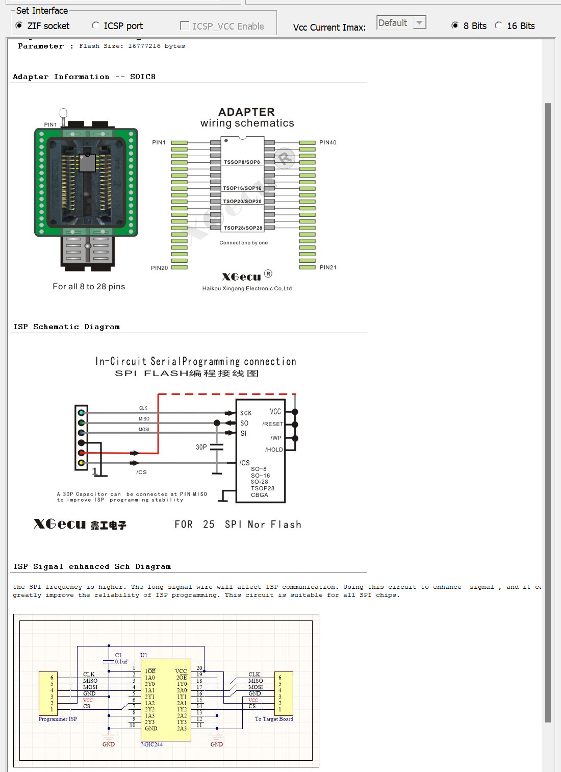
Just don’t forget to do the 3.3v conversion of the CH341A as demonstrated here
For the 3.3v conversion do as shown below, lift the last pin, then solder a wire to the middle pin of the AMS 1117 - Voltage Regulator and soldered to the capacitor, then solder in the lifted pin
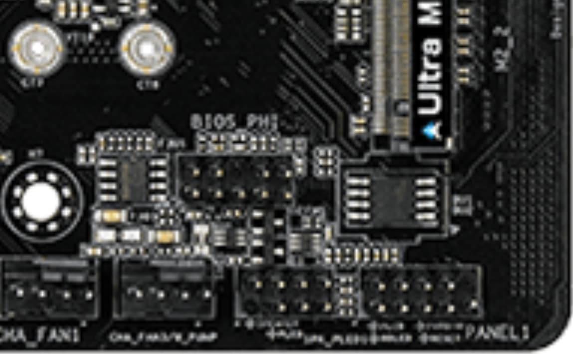
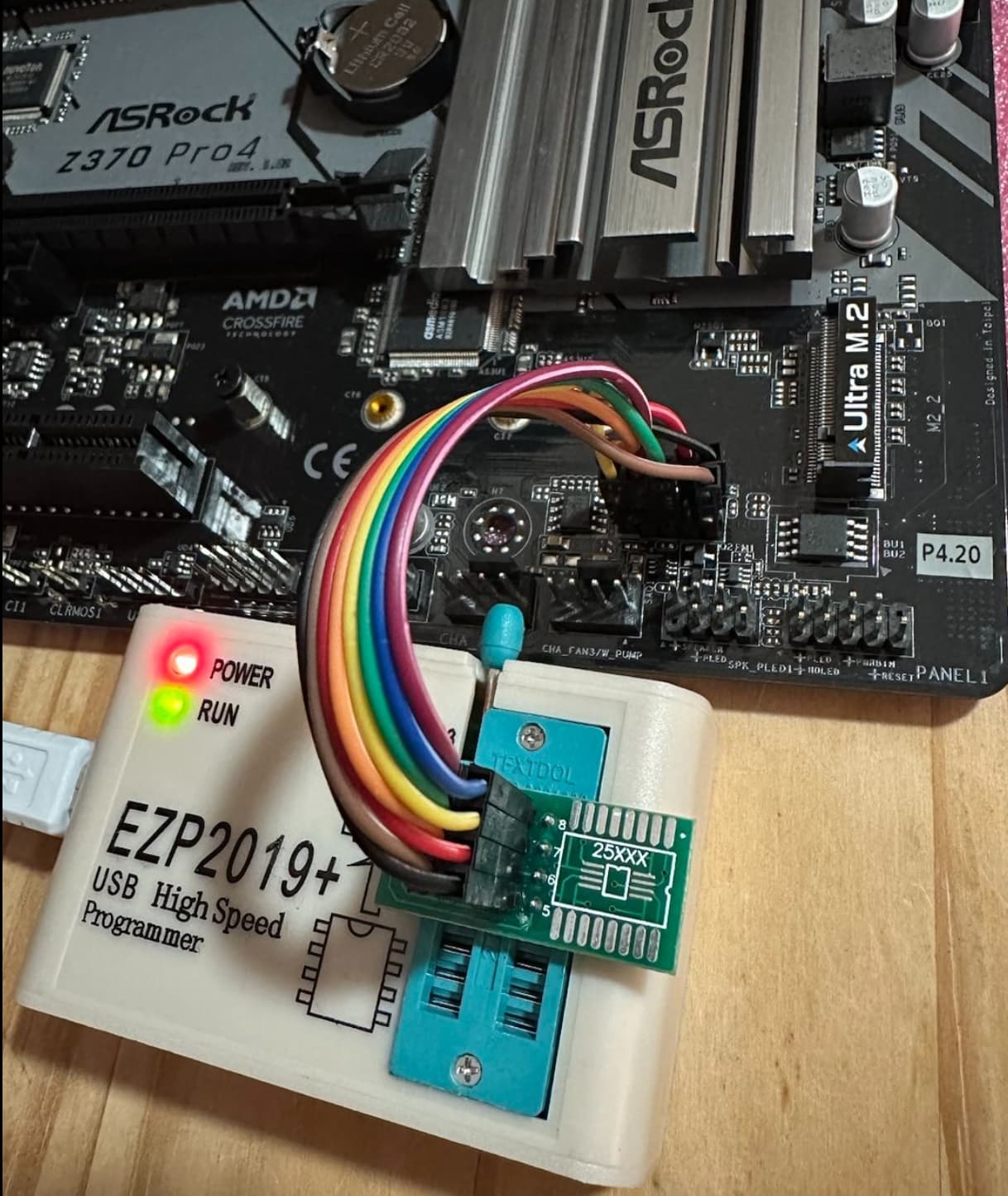
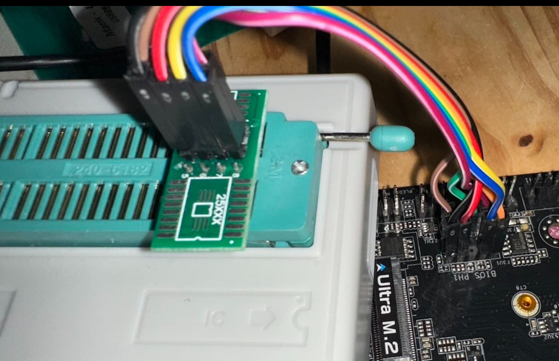
I have the exact same problem but on an AsRock z370 Motherboard while plugged into the BIOS_PH1 header
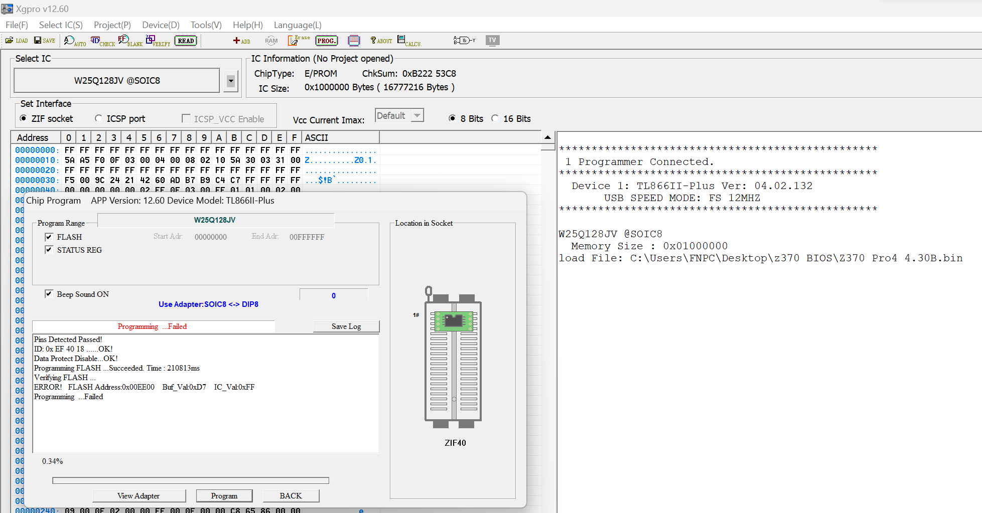
My programmer was reading it in a really sketchy way (some stuff at the start then mostly Fs), then it did write a new BIOS image but would return an error during confirmation.
Other times my programmer would simply get stuck “erasing” the BIOS chip forever in a loop.
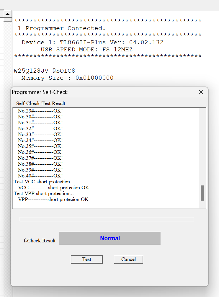
I am using a high-quality programmer called XGecu TL866II Plus. So it is not the programmer’s fault.
It autodetected the BIOS chip correctly so it is not that either.
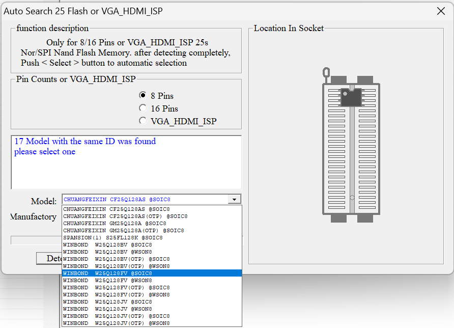
When it detected the BIOS chip by ID it does show multiple chips with the same ID.
Some are
“SOIC8”
“SOIC8 + OTP”
“WSON8”
“WSON8 + OTP”
I am not sure if this “OTP” variable is the problem.
I have the exact same problem but on an AsRock z370 Motherboard while plugged into the BIOS_PH1 header
My programmer was reading it in a really sketchy way (some stuff at the start then mostly Fs), then it did write a new BIOS image but would return an error during confirmation.
Other times my programmer would simply get stuck “erasing” the BIOS chip forever in a loop.
I am using a high-quality programmer called XGecu TL866II Plus. So I hope it is not the programmer’s fault.
It autodetected the BIOS chip correctly so it is not that either.
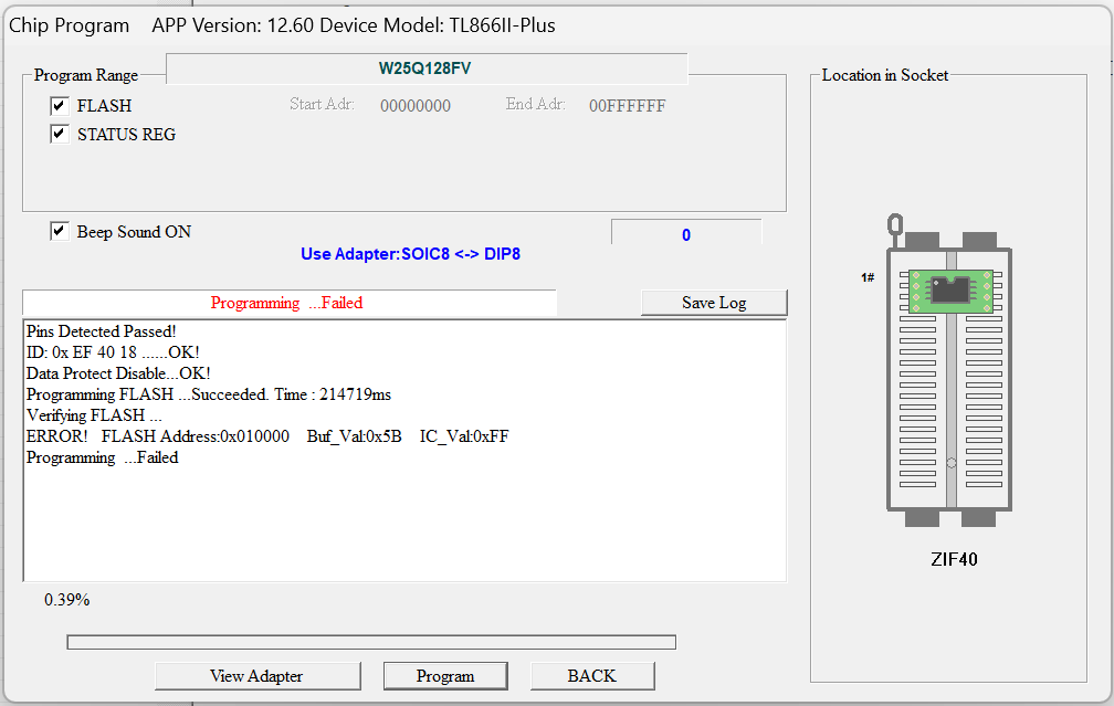
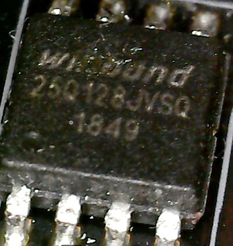
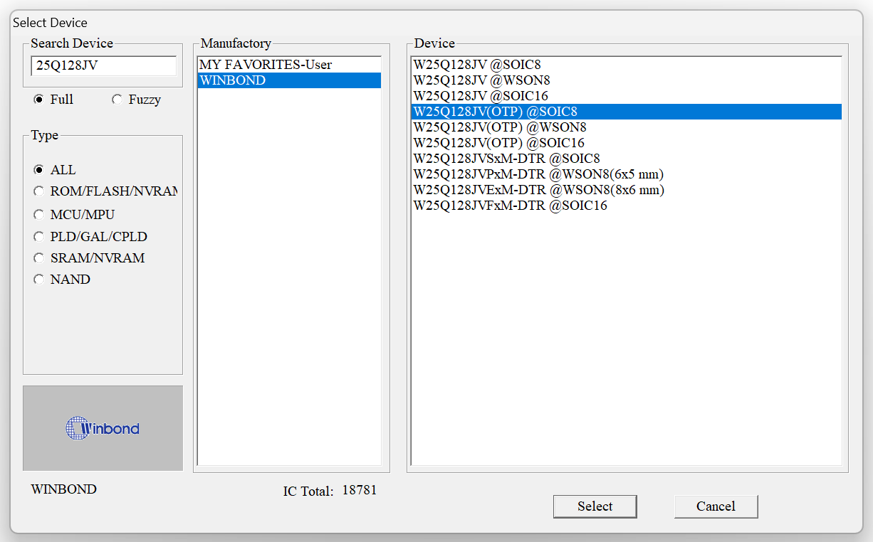
Reading this thread I see the chip “W24Q128FV” in one of the pictures and my XGecuPro software shows this:
So I am guessing this is the correct chip but since it returns the error at the end or it does not seem to be working flawlessly, I was wondering if maybe some of the variants of this chip must be selected instead or of it has something to do with this “OTP” mode or something.
When it detected the BIOS chip by ID it does show multiple chips with the same ID.
Some are
“SOIC8”
“SOIC8 + OTP”
“WSON8”
“WSON8 + OTP”
I am not sure if this “OTP” variable is the problem.
What board are we talking about? Checked some Asrock Z370 board, none of them had bios header?
If you can’t read correctly you almost ever can write either.
.
It’s nice to know what chip the program recognizes but you might want to double check what’s written on the chip (and correct program settings accordingly if not identical)
Next thing is to doublecheck the pinout of the board header and if the cable connects correctly to the programmer!
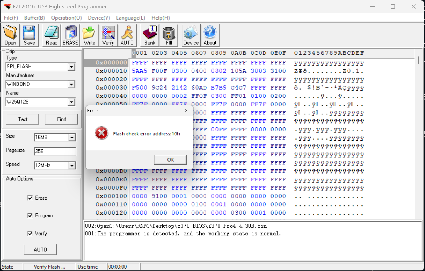
I thought the XGecu was very good, but it I also have this one called EZP2019+ and it appears to be working.
this ch341A trash everybody uses, exploded on me once even after the voltage mod. so i dont buy that. lol.
The header does not appear in the manual, it is only possible to see in the real images of the board, which are very low-resolution. But there it is. I plugged it in correctly based on another thread called
“[CH341a Problem] Which bios_ph1 Cable for ASRock Z270 Pro4?”
The thread is correct the connection does work for me but it was the programmer or something. I am still waiting for the EZP2019 to finish…
Firts of all… we dont know if you really, visually identified your SPI model…
Second…Asrock Z370… very accurate.
Third…the usual mistake as always… no stable/correct reading, then NO NEW FLASH… general rule, if the reading fails the write cant be successful.
EDIT: MERGED, no double posts for same issue, please, thank you.
The chip does not say anything unfortunately so i needed to investigate the forum and the “auto detect” options available
That is literally the name of the board lol, and the title of the thread, but I had not noticed that for the other guy it was z270 Pro4 and not z370Pro 4.
I didn’t know it didn’t read it correctly until too late because it read some parts but not others
Bonus: You merged it into the “wrong thread”. I would have preferred to merge to the other thread but whatever. The other thread is more relevant.
I thought this guy was having the issue with z370, but i later noticed I has X370. they all have names that are too similar so it gets too confusing.
UPDATE:
The EZP2019+ Also returned an error during verification on the same address. So I guess I have a brick now.
My EZP2019+ Programmer only offers “Winbond W25Q128”
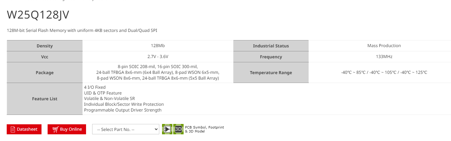
My XGecu does have more specific subtypes and goes up to “Winbond W25Q128JV”
However, my chip also has “SQ” at the end
But unfortunately my XGecu does not get more specifc after “JV”.
I was hoping they are so similar that it should work in theory. But perhaps not. If the latter is the case then there is no way to make it work with my chip because there is no “-SQ”
I have tried with this “-JV” subtype and I still get the same errors
By the cap you show you had the JV and you selected JF and used it to program…
this doesnt mean nothing or it can…it all depends on the apps/prog database and the cmds from it.
The “SQ” is not used here, its usually Package type and special options, read the DS , its all there and recheck connections.
EDIT: No you dont have OTP… did you read the DS?, without reading we dont learn, and the link i provided should had been the 1rst thing to look for after visually identified the SPI before any actions… as you did.
Last tip, some system boards needs psu standby power ON, with or without CMOS battery ON/OFF, over_n_out, good luck.
Yes, Before I used the USB microscope I was using the xGecu “Chip ID - Automatic detection” option and I tried multiple of the chips on the list (that say SOIC8), and they all gave me the same problem.
I think at one point I ran the programmer with the “BV OTP”. So I don’t know if by doing this I possibly damaged the chip. Maybe my chip is now damaged. I don’t know. Is this a possibility?
This whole time I have been trying to figure out if this OTP term plays any role.
“UID and OTP feature” maybe I have to select the OTP variant? I am not here trying to troll you or to make you angry, I am just asking a question. Is this “Can this OTP thing be a possible issue?”
I did try with and without battery but never with any standby power.
I will have to try with the Standby Power, I suspect this is going to solve the problem.
Unfortunately, that was not the solution. I tried it and it didn’t work.
Here is a clue that I want to share as I further investigate my problems
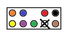
Maybe instead of wiring it into the (Dual In-Line Package) socket I should be using the ICSP port on my xGecu tl866ii plus programmer.
It is 6 pins instead of 8 pins. It is the same pins minus pin 4 (ground) and pin 8 (VCC).
and I can try to use the pins in this thread but then convert into the ICSP version and as show in the picture above in the xGecu support materials.
I can then try to do this multiple ways:
A. Without standby power, without battery
B. Without standby power, with battery
C. With standby power, without battery
D. With standby power, with battery
And just as a bonus for verification purposes, this diagram also uses the MISO MOSI terms. It seems like a lot of different manuals are referring to the same pins with very different terms so it is very confusing. Unfortunately the J3455M manual uses very bad terms that I have not seen anywhere else “DQ0, DQ1, DQ2, DQ3”. So I am trying to do my own investigative work here to actually verify the equivalent terms.
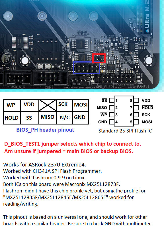
 ) hope that helps couple of you out there, cause even i suspected that the layouts are the same, we only got 1 try maybe and i don’t wanna start soldering a new chip