yes, but that is only during core test. for that reason i keep it at 1200/0.95V and get ~65W power usage while trying to solve memory issue
as you wish. but even with your timing strap i do get gpu errors, and crash at 1900Mhz.
so it is more than obvious this ain’t going to be mem timing problem, but something else.
on win10 (not sure if UEFI/GOP interferes might check that later) with the same bios i get 5W less power consumption and the same furmark test crashes at 1850Mhz. on win7 it passed 20 minutes at 1850Mhz with only 4 mem errors in the best case (win7 - it crashes at 1900Mhz)
from this comparison my suspicion is aimed at memory voltage. most likely it is heavily undervolted even in bios and further in win10…
@karmic_koala You are more than likely hitting the frequency limit but the thing with Polaris is that close to and even at the frequency limit there is quite a bit of scope for timing optimisation which you can only conclude is there simply due to how horribly optimised the timings are to begin with.
3 GHz at 1.35V (unless undervolted) reported as 1500MHz which they are set at stock BIOS. so even if not undervolted i’m sure they can’t go 1800MHz stable. so i’m looking for a way to raise MVDD/MVDDQ. rated as 3.5GHz at 1.5V they should be stable at 1750MHz, i’d expect even up to 1900MHz and maybe give few mem errors at 2000MHz. IIRC others with these Hynix memory modules are able to go even over 2000MHz. VDDCI tried fixed at 1.10V it changes no thing at all. but it looks like MVDD voltage cannot be set the same way as VDDCI. any idea what MemoryTrainingInfo table is used for? i see sapphire cards don’t have it
@karmic_koala those ICs look like they are specced for both 7gbps and 8gbps, which means they are most likely tightly binned parts so I would not automatically assume they will reach 8gbps if the stock speed is 7gbps, 7.6 - 7.8 is likely what you can expect to get out of 7gbps ICs.
EDIT: Did you ever try changing RASMACTRD, RASMACTWR, and WRPLUSRP? You can further iron out memory errors by raising these timings which despite their appearance are in nanoseconds, try 63, 72, 76 respectively.
will give it a try. meanwhile i tried changing spread spectrum settings and it makes no difference. it appears spread spectrum is not even working as i get round-up clocks (e.g. 1200/1500) not like with CPU when spread spectrum is enabled (1400MHz->1397.20MHz)
how do you know the RAM ICs are rated 7/8 Gbps?
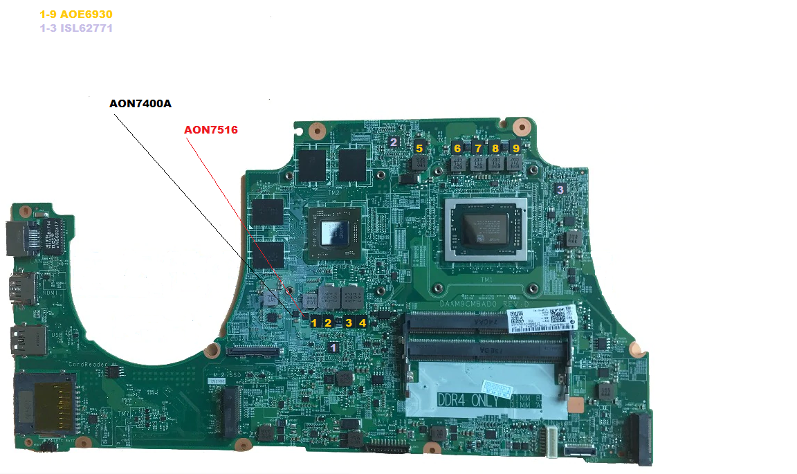
i made some PCB component markups
it seems first ISL62771 is responsible for RX560 core/aux power, that gets fed by 4x 6930 MOSFETs and 2 small 7400A/7516 MOSFETs, second ISL62771 is controlling vRAM and powering via single 6930 MOSFET while 3rd ISL62771 controls CPU voltage and powers CPU using 4x 6930 MOSFETs.
if this is correct i suppose there is a possibility to control MVDD/MVDDQ voltage on this system?
@ket tried it. it is a performance killer and doesn’t help with errors.
Simple specifications the RX560 uses memory rated for 7gbps, meaning you’ll get 7.6 out of it most likely, maybe 7.8 but thats going to be as far as most ICs of that type will go and of course if you are unlucky and have a weak memory IC you may not get past 7.4 or 7.5. You’re getting about 95% of the maximum potential right now rather than chasing those last few MHz it’s much more practical to focus on finding the absolute optimal memory timings copy/pasting timings found on the internet or using PBEs one clik optimisation is not a good way of going about that.
@ket tried it. it is a performance killer and doesn’t help with errors.
You are clearly pushing too hard and too far then, this is doubled down by the fact you say it didn’t help with memory errors. On both an RX470 and RX580 those timings you can safely adjust with zero impact on performance (in fact CU performance actually went up, most likely where the data being sent now has adequate time to be recieved and executed rather than some data having to be fired off again) but again as I have said you need to find optimal timings you cannot just copy/paste what you find I can offer suggestions to put you in the ballpark but it is up to you to find the refinements no silicone is created equal.
i’ve tried to use hynix stock timings for 1750/2000 freqs from desktop cards. even not fully optimized they are still suppose to be stable at these freqs. they give me same amount of errors or slightly less but with worse performance scores, however crashes are present at 1900.
you say RASMACTRD RASMACTWR WRPLUSRP of 63, 72, 76 gave you performance boost? for me it dropped by 2-3FPS. i then took these values from the strap i used and tried to go more tight with these e.g. 48->46. got 20 pts higher score in furmark. negligible difference and not worth the possible further stability issues.
but it seems that the crashes at 1900 are less frequent if i input memory voltage of 1.10V in overdriventool, the thing is that it sets core voltage too. maybe i should just put it at 1.20 or 1.30V for the stable 1900Mhz GDDR5
Maybe I missed it but I wasn’t aware you were undervolting the memory itself, 1.1-1.2v should be plenty for at least 1750MHz but its not the memory you need to be concerned with when it comes to power draw, most of that is exclusively the GPU itself you’ll probably find optimal frequency to power draw around the 1.1-1.15v region. Throwing more voltage than that at the core will just be a waste even throwing 1.25v at it you likely won’t see more than a 50MHz gain at best which just isn’t worth it for a small bump like that and the extra heat and power draw it will generate and the lower temperatures from reduced core voltage will also help the memory out a bit as the ICs won’t get as hot which at the very least will add stability. Optimal stability/performance RASMACTRD, RASMACTWR, and WRPLUSRP is usually 1 strap higher than whatever the values are with your stock timings. Eg; if stock memory is 1750MHz take the RASMACTRD, RASMACTWR, and WRPLUSRP values from the 2000MHz strap. I have no idea why these values are so horribly incorrect with stock timings but stock tiimings as a whole are horribly configured anyway. The RTG division of AMD really are afraid of putting their best foot forward, wether thats through simple laziness or being inept I can’t say but my natural inclination is a combination of both from RTG.
Just as a for instance if RTG paid me to do so I could quite easily improve the performance of their GPUs by 10-15% just because I’ve actually been involved in the memory side of the industry and know what I’m doing, only a fool would scoff at the opportunity to make their products look even better against the competition but RTG are somewhat the fools as for years they have never properly optimised their GPUs, hell, they plain ignore DX9 optimisation, have given up with their Windows OpenGL support/performance despite the community developed OGL driver (RadeonSI / Mesa) absolutely destroying the Windows one making RTG again look like complete amateurs and to really add insult to injury in you are a Windows user is that AMD RTG are still trying to pretend DX11 doesn’t exist which means poor DX11 performance relative to what the cards are actually capable of with a good driver.
as expected, even though i hoped for the opposite, the 2nd ISL and 5th 6930 are used for northbridge not GDDR5… but, left of the 2 big GPU chokes are two smaller ones. the one most on the left appears to be providing power to GDDR5 modules. DMM measured 1.368 idle and 1.362 under load. so it appears i have 150mV free to go up, just need to figure out how. also to add GPU core voltage measured on a capacitor right below the chip was 0.94V while hwinfo reported 0.938V. so pretty accurate.
@ket thank you for the interesting guide. I have a RX 570 with 4GB of SK Hynix vram:
I take both power limits and RAM speed could be approached in a slightly different manner. without stealing your "magic", are there some specific aspects to be aware of? TIA
@elisw everything you need to be aware of is covered in the guide really, if you don’t want to use manual voltages with the card (and thus not keep having to select manual voltage mode in Wattman, if thats what you use) you can instead just use one of the voltage pointers and utilise the offset voltage to attain the desired voltage both with automatic and manual voltage modes. Usually I select an auto voltage pointer for 1.125v as thats around the optimal power draw/frequency in most cases and is certainly better than the auto voltages throwing high voltages at the card with frequencies that don’t need it that is an extremely inefficient way of doing it and why unless there are tools by the time I need a new GPU I’ll probably go nvidia again, RTG have much to improve upon.
@ket thank you for your help, to be honest I’m new in the GPU optimizations and I notice a few differences between the 580 you have shown and the 4GB 570:
in yellow I highlighted the values that are not in line with the guide: power and memory are lower to start with, so your 126W as minimum max power limit should be lowered. the card has two Vbios(es) and my intention was to have a fully optimized Bios along with the original one.
@elisw As in the guide (or I think I mentioned it, if not I meant to) some cards have quite weak VRMs, below the AMD design spec, so you should not raise or lower their default TDC values while TDP should be adjusted accordingly. The lower memory limit is normal on 4GB 4/570s thats why I stated on 580s the stock frequency is 8GHz (8000MHz effective, or as PBE would show it 2000MHz) Only going to 2000MHz memory strap for Hynix memory is a new one though your card is the first I’ve seen only going to that, doesn’t matter though, just means you won’t have to deal with even shittier memory timings above 2000MHz. What kind of memory optimisation you aim for will depend on if you have a card that can overclock the memory well or not.
@ket you did mention the VRMs quality (about a Powercolor Red Dragon IIRC) but this is a different card: all 570s do have a lower TDP and power usage altogether. What I mean is I doubt any 570 manufacturer will use the same power setting they use on their 580s. this said the card I got is definitively an el cheapo version (although with hynix memory modules, at least), I’ll try with some OC and see. thanks again
@elisw to clarify a little more most 70s and 80s will have similar TDP/TDC settings the most likely occurrences of more significant changes will be with cheaply made versions and versions with one PCI-E connector instead of two. In your case you should be fine raising TDP up to 150w or 225w depending on if you have a card with just a 6 pin PCI-E connection or one with an 8pin. As it seems like you probably have a crappy VRM on the card optimising the amount of voltage the card uses will be vital in making sure the card throttles back as infrequently as possible. To have an idea at what the optimal voltage for your card is use GPU-Z to take a look at the cards ASIC quality, the higher it is the less voltage you will need. Typically 1.125v is the optimal voltage, to make the card use that for both manual and auto voltages you would input 65284 using PBE.
FWIW the card I have has an 8 pin PCI connector, but, reading your guide, my plan was about decreasing voltage and power use, not increasing it. unfortunately I may have to change my plans: Asic rating is 75.3%; better than 38% of similar GPUs (below average then)
FWIW the card I have has an 8 pin PCI connector, but, reading your guide, my plan was about decreasing voltage and power use, not increasing it. unfortunately I may have to change my plans: Asic rating is 75.3%; better than 38% of similar GPUs (below average then)
What I said is correct here, more cheaply made versions and/or versions with a 6 pin PCI-E connection instead of an 8 pin. 175w > 135w is a big difference; 30%. The 570 comes in more expensive flavours just like the 580 which is where your 570s come from with specs and limits almost/the same as a 580 but nobody really bought the more expensive 570s because they were only £/$20 or so cheaper than the 580s at the time but on a hardware level aside from a few missing CUs\shaders they were the same.
Or maybe a better way to explain it; AMD reference 570s used lower spec components and fewer VRMs as they were designed with a lower power draw in mind, all most AIBs did with the more expensive 570s is take a 580 PCB, perhaps leave off a few VRMs for cost saving and plonk a 570 GPU on in place of a 580 GPU, and thus your high end 570 is born with mostly 580 specs, which is what the Sapphire and XFX models there are.
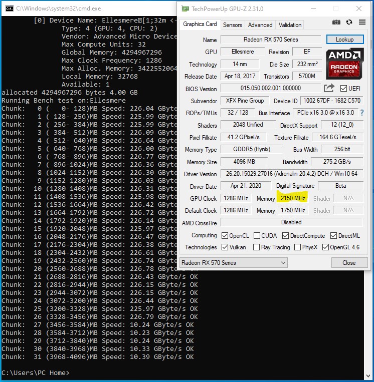
Ok. I did all the homework (up to the intermediate tuning) and managed fairly decent results. The "new" Hynix, although rated at lower frequency do go well with some OC (and do not suffer from the crp upper memory strap the "old" do). 2150 MHz for the vram seems stable (keep in mind the starting point is 1750, not 2000). Unfortunately you have to select the Hynix timings (Memory timing level2) in wattman, if you leave it in Automatic it selects the crppy Elpida timings although GPU-Z recognise the chips as Hynix. standard frequency Hynix timings:
with some OC:
now it’s time to work a bit on the timings, methinks…
what is really important is to unleash some current (power limit +30%) as 112A for TDC is a problem, even at stock settings (I use Superposition as testing benchmark: without the extra current, GPU frequency is not consistent through the test). On the other hand it is possible to perform some undervolting (up to 50 mV reduction). I do not understand the reason behind it, but if I lower ALL the values in wattman by 50mV I get different power results compared to using Afterburner with -50mV (about 160W with Wattman, 135W with Afterburner) while retaining the same OC performance at 1.43GHz. Fan profile obviously needs some tweaking to keep tempeatures at bay. @ket : I edited all the straps from 900 upwards (I didn’t like to have more relaxed timings at lower frequencies), using your strap and the existing lower straps as guides. the 2k (last) one turned out like this: 7770000000000000228E9D0073EE8D53B06914153ECF560C004E26017E0514206A8900A0020031201C143F48C5324C1A opinions? It is a tiny bit more relaxed than yours but I wanted it to blend in with the existing ones. In case things turn pear shaped, I will take the safer 9-9-9-9 route
for anyone looking to up their VDDCI voltage there are 2 ways that work on RX560
first one sets the static voltage value that is varied only by LLC/Trim offset settings
the value defining VDDCI is in ASIC_Init table 02 05 02 04 00 6B 03
second way is more convenient as it doesn’t even require BIOS mod since it can be applied to registry.
it involves modifying platform capabilities field, contained within powerplay table, defined in pptable_v1_0.h as ulPlatformCaps setting bit 15 enables dynamic VDDCI voltage and the VDDCI values from memory table are then used for each memory state respectively
Good info there, you might want to run some tests with that registry method though as its possible to make the driver BSOD when the card comes under load if the expected VDDCI isn’t returned true. RTG tried REALLY hard to stop people from modding Polaris cards… god knows why its us modders that have done the jobs RTG couldn’t be arsed with doing properly.