@elisw memory is detected at boot when the card poweres on with the rest of the system you shouldn’t be needing to touch anything to do with the timings in wattman, wattman is also a buggy POS I’d basically ignore anything it tells you, use it to set your power limit and disable zero RPM, then never bother with it. Sometimes the driver nerfs and confuses itself when you apply a lot of BIOS level changes and/or try too many different memory timing straps so a clean uninstall from safe mode using Display Driver Uninstaller might be in order. To reach 2150MHz the card you have might well be fitted with 8gbps ICs as thats extremely high for 7gbps rated modules. As for your timings, they are ok but probably quite a lot of wiggle room for improvement, all of the sequential ras timings are rather loose, TR2W is a little loose too, TRP_RDA and ACTRD are on the loose side as well, you’re on the right track though.
Side note: The XFX BIOS on your card might be a limiting factor historically something has always been fubar with XFX BIOSes from my experience, I had 4830s I had to cross reference and flash with an Asus BIOS because the XFX one made the system BSOD when crossfire was enabled, and I had a 290X that XFX threw so much voltage at the card might as well have been a literal open fire touch that sucker even for a second you would get a nasty burn. All that voltage didn’t even help the card OC better, unsurprising considering the inferno it was with XFXs "optimised" settings 
bad news… it seems like there is something going wrong.
the flashed BIOS is not seen as fully working, AMD software doesn’t see it and GPU-Z shows something broken.
below the std bios (left) and the modded (right) with all the data missing.
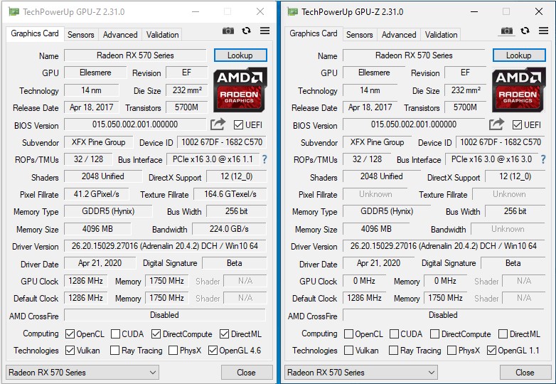
I tried all options to no avail (reinstalled drivers, DDU and all that).
It seems even if I change one single parameter in PBE it breaks it. Even changing TDC from 112 to 115 is enough to break it. any value edited is a failure.
Only thing on PBE that doesn’t break it is the checksum correction after editing the file with HxD (BTW, the bios already has POLARIS20 instead of ELLESMERE, so the only change to be done is from 0F to 07)
Edit:
there is a patch program that needs to be run. I didn’t know about it, once I found out, it works
no BSODs noticed during the valley/furmark tests, or playing UT4 for several hours.
do you know if the system BIOS I2C settings are related to video BIOS I2C configuration? i have I2C 0 - I2C 3 in "SB I2C Configuration" under chipset/southbridge, with only I2C 0 enabled by default
From my experience I2C is flaky, trying to read the information leads to the driver doing all sorts of weird things until you reboot so I’ve not really bothered with it much. Just can’t be arsed with dealing with the dodgyness of AMDs drivers.
how about the situation when afterburner does not detect any i2c devices? disabled by driver/bios somehow? other than that i haven’t noticed anyone mention he changed switching frequency over SVI2. basically all there regulators are based on intersil technology so they might have more in common than it seems
@karmic_koala I haven’t used Afterburner myself as I can’t stand the clunky UI of it I just directly edit the BIOS getting to the metal just avoids numerous potential issues and quirks. You’d be able to get an answer to your question though from Unwinder, I think he hangs out on the guru3d forums mostly these days.
well i guess the i2c method is pointless here, as the damn regulator itself has no SCL/SDA lines at all. from what i understand it is actual regulator that should be enumerated on the bus (or in afterburner or any other i2c scan tool)
AMDGPU devices that linux probing method discover are irrelevant here (and there are no actual slaves on them at all)
so no way to change switching frequency which is suppose to help with mem errors according to Vento041 on oc net, but then again, the regulator has nothing to do with MVDD (at least it appears so, unless VDDIO line is involved somehow) so it doesn’t matter if its 300, 400 or 800 kHz (looks like it is 400 by default according to 34K resistor)…
Hey, could someone please take a lot at my straps, perhaps it maybe improved. Im running at 1975mhz(7900mhz) not usual samsung chips on my rx 580 (K4G80325FC, as oppose to "normal ones" K4G80325FB) 555000000000000022CC1C00CE616C47D0570F15B48C250B006AE7000B031420FA8900A003000000190F2F39B22D3517 .Thanks<br /><br />Edit : Ive been trying to improve my straps, but I cant even go pass 1800mhz even though those straps are more loosen than before. What am I missing, did i messed some formulas, I cant figure it out. 777000000000000022EE1C00106A6D50D057111537CD160B006C070124081420FA8900A00300000019143846B135461A
@Ellertis Samsung memory generally does not clock well on Polaris and will top out at about 2100 (8400 effective) at best. You can make up for the lack of overall frequency with tight memory timings though which will get you 90%~ of the way there in games compared to other memory ICs and you’ll have CU performance thats through the roof. The flipsides however are that you won’t have the same raw speed that some games\engines like which will show the shortcomings cards with Samsung memory have (Alien Isolation is one game that comes to mind where a Samsung based card will get convincingly beaten by a card with Hynix memory for instance) and you won’t quite be at the same performance level as other fully optimised cards overall from a gaming perspective.
Even as someone who is familiar with 90%+ of all the memory timings Polaris uses (sans some architecture/memory controller specific ones) from my time spent in the memory industry it would take literally hundreds of hours to come up with some perfectly tuned Samsung/Hynix (not Micron as I don’t have a card with Micron to test with) memory timings as my personal testing is far more stringent than typical standards, timings must pass a full 24hr test at above stock memory frequencies without a single EDC error @4k resolution with the frame buffer completely loaded and be optimised to perform extremely well in multiple scenarios (mining, gaming, OCing, etc) while also improving upon stock stability (which isn’t actually that hard, RTG were/are just lazy). I could do it for you without a problem, but I’d have to ask something for the sheer amount of time involved doing it and of course that latter point about memory OCing is always subjective based on multiple factors I can’t control but you should none the less see the maximum stable frequency range extended. This is all done without severely crippling efficiency of course, and in fact improving it, no point in all the work otherwise.
@karmic_koala correct the default switching frequency is 400KHz, increasing it will not directly help improve memory errors however it is possible increasing switching frequency would have the side effect of helping with memory errors due to as I’m sure you already know higher switching frequency = a cleaner power delivery signal, but at the cost of working the VRMs harder and thus more heat. Optimal frequency will depend on the specific VRM but for most would likely be between 550-625. The main advantage of a higher switching frequency though is to coax a bit more out of the GPU itself but I never could work out if it was at all possible to add something to the Polaris firmware to set a higher switching frequency on an NCP81022 or IR3567B.
yes apparently you’d need to add I2C object in VOI - it was discussed in the thread https://www.overclock.net/forum/67-amd/1…-memory-oc.html
but in case of these most used regulators (IR, NCP) it appears they’re at disadvantage if used for memory voltage control directly as their performance drops with temperature increase.
on the other hand, there are cards that have separate regulator for memory, this is also case in my laptop, and the memory regulator is not even covered by heatsink, for the obvious reason again, it’s counterpart from alpha&omega (identical pinout, only lower output current 6A vs 10A on the one i have) working temp is rated up to 150 celsius. i’m using this alpha&omega part as a reference since it has detailed information in datasheet while the actual one in my laptop has only one page of specifications
it seemed at some point that i had noticeably less errors when powered on laptop after it completely cooled down (e.g 1-2hours) but after more repeated tests it turned out the heat had nothing to do with it. the regulator working temperature specifications confirmed that and i even tried to do more tests with a small fan from old laptop put just below the memory VRM - there was no difference at all regarding mem errors. a temperature difference of about 20 celsius down was observed on system RAM that is just nearby the GDDR5 VRM so the extra cooling was definitely mounted properly, but as i said, without an effect on GDDR5 VRM or memory performance
I`ve finished messing with memory timimgs, satisfied with the result. Thanks to the author. When i got to VDDCI hex editing… well… I got a bit confused. Is there an easy way (a software), to know the exact IMC that is on the PCB? Thanks
Assuming your VRM is rated for 150c I wouldn’t expect to see any stability improvement with it being actively cooled unless the VRM was already nearing its limit, say 130c. Anything up to 100c you are going to get about the same stability-wise the active cooling is just providing the benefit of keeping the hardware healthier for longer and if you are under 100c full load on that VRM you really don’t need to cool it at all but it really does depend on the quality of the VRM if it is a mediocre one with a limit of around 120c or a crap one with a limit of around 100c I’d definitely be looking at ways to actively cool it or at the very least use high grade thermal materials, heatsink it and get some sort of natural airflow over it.
@Ellertis usually we just do an I2C dump but in your case the easiest way would be to remove the cooler and just look at the chip itself. You have a XFX card if I remember correctly? Its probably an NCP81022 if thats the case, XFX cut every corner they can with their cards. If you don’t want to remove the cooler you can open your vBIOS with SRBPolaris, go to the voltage tab and if there is a dropdown for voltage offset congrats you have yourself a card with the IR3567B, if theres no dropdown you likely have the NCP81022. Whats the strap for the timings you ended up with? There may be a few quick edits I can make for you to get a little more out of it.
As a side note I have noticed all the RX580s and 470s I’ve tested seem to have one thing set in stone; once you reach in the region of 223-225GB/s you are at the upper limit of the bandwidth efficiency the card can handle before EDCs start creeping in. At that point you don’t have to push for higher bandwidth though as you have eliminated any bandwidth performance bottleneck the GPU would need to be getting close to the 2GHz mark to even begin to start threatening to be bandwidth limited again.
Also fun fact: with bandwidth around the 220GB/s mark compared to an RX590 that bandwidth improvement is making up a GPU frequency deficit of about 150-200MHz. EG; An RX580 @ 1.45GHz and optimised stock memory timings is going to be at the same performance level, perhaps slightly faster, than a stock RX590 with a GPU clock of 1.55-1.6GHz.
no stability from additional cooling on GDDR5 VRM, but increase of voltage to 1.53V got rid 95% of mem errors, just played UT4 for more than a half an hour at 1200/1800, 0 errors!! valley test sometimes give a few errors and sometimes passes at 1200/1900 with 0 errors.
so definitely MVDD/MVDDQ voltage increase helps, and regarding VDDCI i see some people’s hwinfo screenshots with AUX power of more than 100W, unless their cards are wired with core phase on AUX rail that is huge power waste as i don’t see no performance improvement with raising VDDCI, on the contrary, undervolting it to 0.80V (min stable was 0.65V) helps keep GPU cooler.
also got 240W PSU meanwhile and it helped with system crashes when GPU is under full load and CPU running with PowerNow disabled.
and managed to understand 99% of mess in bristol APU powerplay table: https://github.com/sibradzic/upp/commit/…omment-40017876
and won the UT4 godlike deathmatch against 23 bots at deck16 and godlike CTF at facing worlds in the same night 
@karmic_koala I tried finding memory voltage in a few different RX580s and 470s, never could find anything conclusive perhaps you would have more luck on that count. Would be pretty cool to be able to run TRRD 4 or 5 and TRP_WRA 50 and TRP_RDA 26 @ 2150MHz+ with 1.55 - 1.6v bandwidth on a 580/70 would shoot up to around 232-235GB/s when combined with the other optimised timings and give Polaris one final shot in the arm picking up most of the terrible coding slack on the driver side which depending on what type of RX580 you have would take it to above GTX1070 levels of performance in a lot of cases. To this day I still can’t understand why AMD didn’t move Polaris for the RX590 to a 9nm node (even if it meant waiting an extra few months) and at the very least upgrade the memory frequency to 9Gbps especially as AMD are so insistent on 8GB Polaris cards still being relevent midrange cards to this day… they aren’t, not without the extreme tuning you’ll find here.
I also used to play UT99 GOTYE back in the day ![]() I absolutely rocked at it. UT4 is alright but the modding community never really picked it up and without awesome (and hilarious) weapons like the proxy mines and un-nerfed UT99 style weapons damage the game just doesn’t feel the same to me nor is it as fun. There was method and strategy still amongst the chaos UT99 had, not such thing with any UT game since
I absolutely rocked at it. UT4 is alright but the modding community never really picked it up and without awesome (and hilarious) weapons like the proxy mines and un-nerfed UT99 style weapons damage the game just doesn’t feel the same to me nor is it as fun. There was method and strategy still amongst the chaos UT99 had, not such thing with any UT game since ![]()
@ket this is actually RX560 chip, so only 3000M transistors inside vs 5700M on desktop cards and close to 50% less of performance is expected due to this.
haven’t really played with timings yet (found some tools that do it on-the-fly, one time it changes timing, next time it changes and reverts it so didn’t want to lose my patience with it) but managed to go as high as 2100MHz on memory while running oclmembench, unstable, one test passed another crashed system. will try to drop more volts at the RAM later, GPU core current seems to be limiting factor too that plays its role regarding memory errors and that one i’m currently trying to figure out whether is hard limited or somewhere in bios.
just ran one oclmembench test with 1560MHz core and 2080MHz RAM, GPU-Z reports theoretical mem bandwidth of 133.1GB/s and measured bandwidth was 116.5GB/s which is 87.5% so i think efficiency is near the top already
UT99 i also played some 15y ago, haven’t checked the 2003/2004 releases, but i think UT3 was (regardless of the online reviews) their best release till now, first thing that leaves impression in UT3 and you can’t go without noticing it is absolutely unreal graphics across gaming arenas, and also bot taunts are hilarious…
87.5% is pretty high, on an RX580/70 its about as high as you can go without increasing memory voltage. Not sure if this limit is architectural or just voltage but I’ve tested 3-4 cards now and they all topped out around 221.5GB/s before EDC errors started creeping in and thats regardless of if the memory was at stock or OC’d so definitely some kind of hard limit. Now I’ve found the absolute best performance with the memory OC’d I might set it to stock and find the best performance in theory you should be able to get better performance at the stock memory speed but some games like frequency more so its swings and roundabouts best timings at max OC is the best of both worlds.
.
You actually need to do both, offset values will "override" automatic voltages but you still need to set manual voltage values that compensate for the offset value. Eg; auto voltage is 1.2v, manual voltage in Wattman is 1.1v, but your card only needs 1.1v for the maximum GPU clock it can handle. You would need to set offset to -100mv then use manual voltage values +0.1v higher so you still achieve 1.1v regardless of if you use automatic or manual voltage. AMDs automatic voltage algorithm is completely messed up, regardless of measured ASIC quality (which the vBIOS is actually aware of) the automatic algorithm is +10% of the required voltage to account for OCing (which is stupid, thats what the manual voltage adjustment is there for) + a bit more on top of that (2.5% or 5% I believe, can’t remember which) to account for electromigration over time. This can lead to the GPU having as much as +0.15v (thereabouts) more than it actually needs which may not seem like much but under load that just means more power draw, extra heat, more fan noise as they need to spin faster, and more wear on the graphics card itself. Regards the baseline 300MHz 2D clock there is a minimum bar set that won’t let you go below it in the usual method, that lower limit is 0.75v. Offset voltage will like everything else override it (or it always has in my tests on several different cards, put it that way)
can’t really understand this 69.727A core current limit… it definitely appears to be crucial for the better effective core clocks and maybe as a side effect less memory errors but what is limiting it? TDC values change in clocksource table don’t help as it first seemed, instead looks like they are used only to adjust reported power reading bias…
i thought it might be VRM limit and tried to contact buildzoid to get a better opinion on the issue but haven’t got any reply yet
so i tried to find other GPUs that use E6930 MOSFET, and there is GTX 1060 6GB card reviewed on tomshardware that has these same VRM modules, more precisely that one use 3 true phases with only one such MOS per phase (for both low and high side) in their test it reached about 120W at 1.05V
in my case there are 2 true phases, with each phase having two E6930 so i thought they are used in parallel, D2/S1 pins of each MOS in a phase are wired together (in theory parallel MOSFETs should increase output current)
worst thing is it is impossible to find reliable info about VRM circuitry, what would be max output given the low/high side specs in each of the operation modes…
e.g. E6930 has even different specs, ones rated against case temperature
low high
Tc=25°C 22A 85A
Tc=100°C 22A 85A
and against ambient temperature
Ta=25°C 22A 60A
Ta=70°C 22A 48A
according to these specs and the fact GTX card can deliver about 114A i’d expect the 70A shouldn’t be max limit here, but not sure as it is hard to verify this without proper info.
even if it turned out 70A is max MOSFETs can provide, would it make any sense to replace them for E6932, this one have following spec
low high
Tc=25°C 55A 85A
Tc=100°C 35A 85A
Ta=25°C 21A 38A
Ta=70°C 16A 30A