Hey all, and specially @Lost_N_BIOS :
I decided to start a new thread related to this two-Socket Xeon E5v2 Board.
I have let this topic aside for a year, but have recently come back to it, and I thought a separate thread would be best.
General questions regarding the Z9PE-B8 WS Board:
1.) How do I write/flash a modded Bios image here?
2.) How can I make use of Intel MEI fptw tool?
3.) [optinal]: Where is the first CPU’s PCIe Root Port1 connected to?
1.)
I have sveral systems in use, based on Intel C602/X79 IvyBridge-E architecture.
With help from the forum I have managed to add recent microcode patches, bitfurcation unlocking and nvme boot options to my P9X79E-WS and P9X79-WS boards.
That is, I was provided with a bios image by @Lost_N_BIOS and was able to write it using the Asus Flshback-Button.
Recently I added a Samsung 970 Evo Plus and set up a new Win 10-System.
This system boots from the 970, even making use of Secure Boot and not requiring the CSM.
Thanks again for that help!!
But now I came back to the Z9 board.
@Lost_N_BIOS made a bios image for that too, but I could not get it written because it failed the security test and the board does not feature a “Flashback”-Button.
That brings me to:
2.)
We tried to make use of the Intel Management Engines tools. But even when I try to read from the firmware or bios region (fptw64 -d bios.bin) , I get an error message:
Error 26: The host CPU does not have read access to the target flash area. To enable read access for this operation you must modify the descriptor settings to give host access to this region.
Is my only option left to use hardware flash programmer?
Or are there any other options I could try?
3.)
This topic is not related to the flashing or modding issue. I did not want to start a new thread only for this.
Maybe some of you have a clue:
The Z9PE-D8 WS Board features two sockets for Xeon E5 oder E5v2 CPUs.
The board features seven PCIe slots, each ×16 mechanically.
Four of them are ×16 electrically and 3 are ×8.
Slots #1 to #4 (from CPU downwards) are related to CPU1 while Slots #5 to #7 are related to CPU2.
Slots #5 to #7 directly represent the CPUs PCIe Root Ports.
Slot #6 connects to Root Port1 (1a/1b), which is the CPU's ×8 Root Port.
According to MB manual, slot #1 features ×16 width which is reduced to ×8 when slot#2 is populated.
Same goes for slot #3 and #4.
So I think that slots #1 and #2 resemble shared resources of CPU1's ×16 Root Port 2, as well as slots #3 and #4 do for Root Port 3.
But where are the resources of Root Port #1?
There are still those 8 Lanes from CPU1's first Root Port left, and I cannot locate them anywhere in the MBs layout.
I found this block diagram:
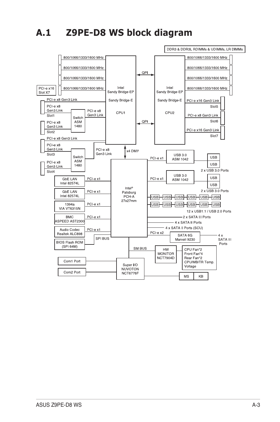
Yet, I can't identify Root Port 1 of the first CPU.
Furthermore, the resources of Root Port 2 and 3 are each shared or splitted - in the diagram they show as four ×8 ports which are provided by CPU1.
Additionally there is a small box in the diagram featuring something labelled "PCIe ×16 Slot X7" which seems to have no function??