Nice. You make a great job. Thank you for all information you provided.
I’m sorry that I cannot answer you all I want.
It’s Chistmas time and I am not at home right now. In few days I am back and I will use your method and read the chip externally. Then compare two files.
I thought about something when reading your last post. My MB has two NICs - i225-V and i219-V.
Did you read my post from yesterday about the OTP area in the flash memory chip of i225-v?
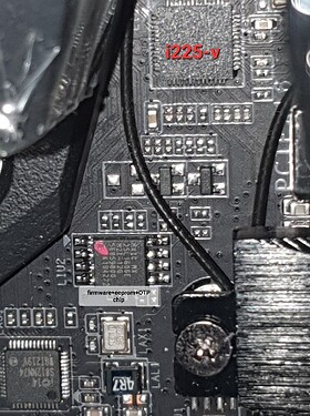
I removed that post today… That card has its own 2MB chip with MAC, eeprom, firmware and 64bytes of OTP (which I’m acually searching).
Here is a copy of that post. I want to show it because I have noticed something in your screenshots.
> Hello,
> Thank you for a possibility to write a topic on a such profesional forum.
> It is my first post here. It is caused mainly by a difficult problem that I believe I’ll get some help here.
>
> Let’s start. Probably most of users heard about issues with the Intel Ethernet card i225-V on a chipset Z490. i225-v card is the 2.5GbE card and Intel suggested all mainboards producers to use that card in their “higher class” mainboards. It appeared that this card has many bugs. They tried to fix them by changing firmware in rev.2, next they released rev.3. People had more and more problems, new bugs were discovered. Then… Intel decided to stop a project “i225-V” and released i226-V. They even did not want to fix them. On my mainboard there is a second NIC Intel i219-V rev.11. I225-V had only 3 revisions. They had to find a really big bug in the architecture of that card.
>
> I have the mainboard Gigabyte Z490 Vision D. My 2.5Gbps NIC is i225-v rev.2. I didn’t need a speed, etc. Just stability. I updated the firmware to 1.45. All producers released that update. Intel claimed that this firmware will solve all problems… But since a first second there appeared next problems. The firmware could be updated only on the old drivers. Fortunately for me, everything went smooth. As I said, I wanted stability, not speed. I never measured its possibilities. Before updating NIC worked quite good, after also. Everything was OK for 2 months. Then the card started to loose some packets every 30 seconds. It looked that way (as example): I was reading news and clicked 4 articles to open in new tabs. 3 of them appeared imediately but 4th not. To open that site I had to click F5/refresh. Even refreshing after “0.01s” worked. Day by day it was anoying me much more. Finally I decided to do something with it.
>
> I found newer firmwares. I believed they are for rev.3 but unofficially I got an information that they are universal. There were version 1.57, 1.68, 1.7?.. I updated the firmware to 1.57 version and my problem was gone. It satisfied me and didnt update to higher version.
>
> Small info about i225-V. It is a normal IC with firmware located on a flash memory chip. The firmware’s size has about 400KB. Asus uses 1MB flash memory chip. Gigabyte uses 2MB flash memory chip… almost 1.5MB are zeros. From 0x100000-0x200000 are only zeros…
>
> One day I had a lot of free time. I wanted to find the reason of loosing packets in 1.45 firmware. Few weeks before I read that Gigabyte had put in factory the i225-V eeprom with the wrong checksum and someone provided proper values (look at Google: hackintosh gigabyte z490 i225v fix).
> I thought it was needed to run that NIC card on hackintosh and nothing else.
>
> I prepared tools to analyze files. I dumped 1.57 and compared it to my backup of 1.45. And my “everything” dropped down…
>
> Quick info:
> The backup has the same size as flash memory and is 1:1 copy. It looks like:
>
> [eeprom—
> eeprom—
> firmware—
> empty_space—
> some_bytes—
> empty_space]
>
> The firmware update file also has the same size but looks like:
>
> [generic_eeprom—
> flash_app—
> firmware—
> empty_space]
>
> … 1.57 dump looked:
>
> [eeprom—
> eeprom—
> firmware1.57—
> empty_space—
> some_bytes—
> empty_space—
> firmware1.57—
> empty_space—
> some_bytes—
> empty_space]
>
> I knew that something is wrong. (BTW. updating to 1.57 was not easy. My language skills make it impossible to describe tricks and fooling software that I used in that process. I’m sorry.)
> When I set Intel app in recovery mode and provided the link to my backup, I saw “incorrect checksum” on the screen.
> I connected everything together in my mind. Because Gigabyte provided mainboards with corrupted checksum of i225-v firmware, now Intel’s app recognized it as the incorrect backup.
> Probably also, the wrong values in eeprom caused double flashing of the new firmware.
>
> The correct firmware starts at 0x2000.
> My second copy started at 0x7D000.
> In that place there should be zeros.
> “Some bytes” I mentioned above were couples of bytes but they were in the places which suggested that they are not random at all. Like 0x76000, 0x7A000, 0x7C000, and few more.
>
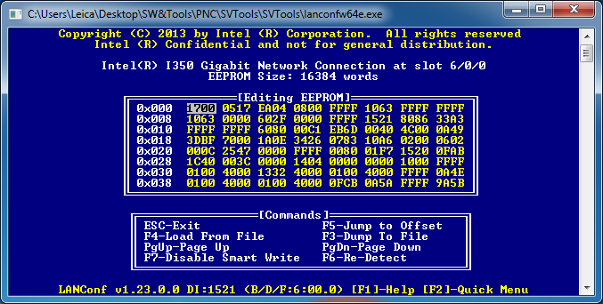
> Writing in eeprom corrected values didnt help. I was so upset. I ‘borrow’ from China the latest as possible apps eeupdate, lanconf, celo. They were in the versions which saw all new Intel NIC including i225-V.
>
> Warning: Those programs are too dangerous. Please don’t look for them if there is no reason! (They allow to modify raw eeprom [but you cannot change every values - the main unit will modify other values to keep the proper checksums - your changes will be rejected if there won’t be the way to make it]. They can modify values of everything - registers, the way of the connecting with BUS. One wrong number and your device is bricked. The huge part of changes cannot be reversed. Furthermore, you can change (the app allows to fool itself) a VID value of any device connected to the PCIE BUS (temporary). For example I can set VID of DDR4 controller or WiFi card to 15F3. That value is the real VID of i225-V. From that moment, the app would see those devices as i225-V card and allows you to see and modify found parameters. Fortunately 95% of devices on the BUS are secured and don’t allow you to even access them at this level. But still about 5 devices access you to mess their PCIE parameters. It is too dangerous for those devices to play with that apps unless you know exactly what you want to do.
>
> For example: Searching the way for remap the flash chip, I changed “writing style” from Atmel to SST. Now SST mode is shown as default. I can change to Atmel but after reboot, SST mode comes back. So you can see how easy is to set the unreversable option. BTW. How do you think, where that change was saved? In the eeprom of the main chip? Did someone discover the method of communication with this 48legs bug-bucket chip?
>
> I made almost 100 different prepared flash files trying to step by step get back the flash memory to the normal look. The funny thing is that card was still working all the time. Despite using so powerful programs like lanfconf and eeupdate, the card blocked every try of flashing. I found the way to bypass that. After dozens of flashing tries with on or off different security options, the card started to work so slow (responses after 20s from commands) that it was possible to write 3% of the flash memory with the other flasher. That means eeprom and the begining of the first firmware. Modifing values in eeprom allows me set the adresses where the main chip of i225-V wrote firmware…
>
> I managed to save parts in different ways:
>
> [eeprom1.45—
> eeprom1.57—
> firmware1.57—
> empty_space–
> some_bytes—
> empty_space—
> firmware1.57—
> empty_space—
> some_bytes—
> empty_space]
>
> [eeprom1.45—
> eeprom1.45–
> firmware1.57—
> empty_space–
> some_bytes—
> empty_space—
> firmware1.57—
> empty_space—
> some_bytes—
> empty_space]
>
> [eeprom1.57—
> eeprom1.45–
> firmware1.45—
> empty_space—
> some_bytes—
> empty_space—
> firmware1.57—
> empty_space—
> some_bytes—
> empty_space]
>
> [eeprom1.45—
> eeprom1.45---
> empty_space—
> firmware1.57—
> empty_space—
> some_bytes—
> empty_space]
>
> (!) Finally I saw in latest dump:
> [eeprom.1.45—
> eeprom1.45–
> firmware1.45—
> empty_space–
> some_bytes—
> empty_space—
> firmware1.45—
> empty_space—
> some_bytes—
> empty_space]
>
> Eee? What the hell? Why the main unit after reboot*
>
> *(the most important in reboots when playing with Intel’s NIC is unplugging a cord from PSU or turn it completely off with button OFF/ON on the PSU for a few seconds. Of course it depends of the components - some PSU are able to hold the energy in capacitors for the longer time. Especially if there is only the mainboard without any add-in card (GPU from CPU). It is not strange to have a power indicator diode on the mainboard turned on for a half a minute. To apply changes in the Intel’s NIC, you have to wait till such the diode turns off [try to power on your PC - fans will move a little and the energy in the circuit should be gone  ].)
>
> did’t erase the second firmware? (The main unit was removing all unnecessary data after the reboot) All other values on the memory flash was the same like in my backup. I thought that eeprom contains all needed adresses. But I was wrong. Or I hit the next bug...
>
> I probably tried all combinations of my ideas but I couldnt find the way to get rid of doubled firmware. Lanconf was showing that the flash chip is divided into ‘2 partitions’… whatever it means. I was not able to change their settings by any option or prepared dumps. IMO those ‘partitions’ was for 90% the reason of that mess.
>
> I don’t remember exact values but it is not important now.
> When lanconf analysed my backup file, it shows
>
> part 0KB (0x0 - 0x2000)
> part 480KB (0x2000 - ...)
>
> The doubled firmware gives:
>
> part 480KB (0x2000 - ...)
> part 480KB (0x7D000 - ...)
>
> So as a real man, I took a hammer and unsolder the flash memory chip. External dump was the same as the internal one.
>
> I don’t know why I did it at night. I was so sleepy. I unsoldered it by a hot air but didn’t even looked at the temp. Next day when I gently read the chip. Next I wanted to write my backup to it but then 6 legs out of 8 felt down. They were so fragile… and yes… Temperature. Please do not comment that. Gods will. I ordered the same chips, the old one went to the electric waste. 3 days later I got the new chips at home. I flashed my backup, checked it in few apps. One app when recognized that chip, but shows two tabs. One app out of 7. (?) Chinese sh*t I thought.
>
> 5 minutes before soldering it, I opened the datasheet. Everything seemed to be OK. Last time I wanted to check voltages to be sure.
>
> And suddenly. On the same page. Almost the first sentence. 16Mbit nor flash memory with 512 bits of OTP…
> Now I don’t know what to do. Because of the temperature, pads probably can survive one last soldering, so I would rather be sure soldering the chip.
>
> 64 bytes. 64 hex numbers.
> Maybe that area is empty?
> Maybe it is especially made for i225-V?
> Maybe it is made for specific model of the mainboard or manufacturer?
>
> This is my ask for you. If someone know what should be in that area, or have a full dump, please write to me. I will pay as much as you want. Software dump can be also helpful to check my 1.45 backup if it has the same structure.
>
> Maybe someone saw values or can check in the other Gigabyte z490 mainboard? And somehow it would be possible to guess the correct values for my MB. Or maybe someone has an access to damaged Gigabyte mainboard with that NIC card?
>
> Two things that bother me. On all other mainboards there are memory chips with small additional OTP areas for i225-V… Low chances to just without any reason.
> And the second: that area can be read only by an external programmer I think. I met some people who want to help but unsoldering the chip was above their abilities and the will.
>
> In that one app which showed me the second tab for OTP memory (and have to find it if offers to write OTP as simply as the standard data), the area of OTP was in a range 0x200000 - 0x200039.
> That memory chip is MX25L1606E.
>
> Thank you if you read that story. If someone can help me, the cost plays no matter.
>
> I know that there is a second ethernet card on my mainboard. But it became my master goal. And I am sorry for mistakes.
>
> PS. You don’t believe how simple I could fix that. I will write it, maybe someone has the same problem or someone’s card stopped to appear after the standard firmware flashing procedure.
>
> There is possibility to make a short circuit on the pins of the memory flash chip (but don’t forget to measure the voltage and current before and read the datasheet. Check if you can do it without risk of burning the chip. If not, just unsolder one leg (vcc)). When the main i225-v chip doesn’t see the flash memory chip then it appears in UEFI and OS with changed VID to 15FD and the name “i225-V without NVM image”. If you unsoldered the pin, now solder it. If you made short circuit then 1 second after turning on PC just stop. Now you can use every Intel program. The card will be visible for all of them. I suggest to make backup first and see what happened. If you have a backup, just flash it. If on the chip there is untouched eeprom, you can just execute the firmware updater (only remove from the script the line that check current version).
>
> So it looks like that i225-V cant be bricked by flashing firmware. With the bad firmware, the card disappear from your PC. But it is fully operative (for fixing) after not detecting the flash memory chip during the start.
> The same situation is when you put the empty memory chip. NIC starts in “factory mode” and waits for a flashing command. Good luck.
>
> Best Wishes
I use a mobile phone for writing… I hope it would be readable…
What did I notice on your screenshots?
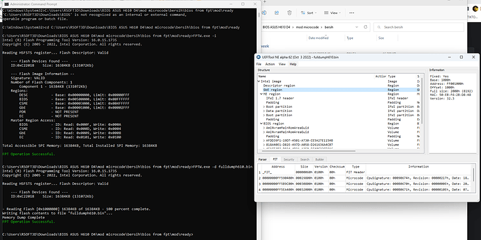
Your ‘SPI BIOS chip’ has the ID 0xC22018.
It is the MX25L12835E chip… in its datasheet we can see:
SOFTWARE FEATURES
- Flexible individual block protect when OTP WPSEL=1
- Additional 4K bits secured OTP for unique identifier
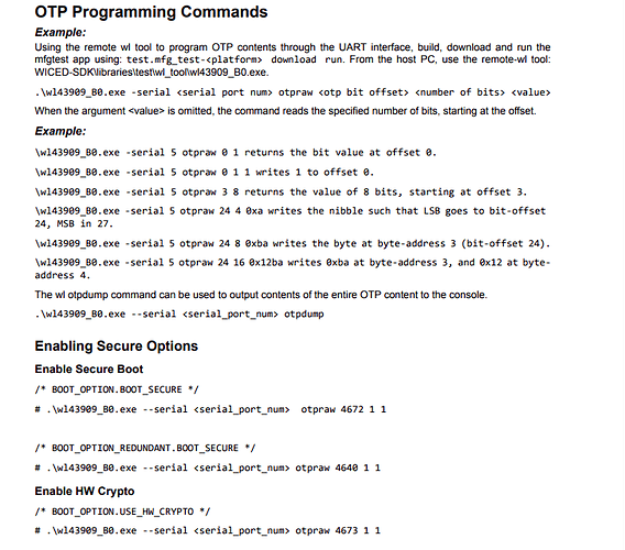
What that means? It is a similar ‘problem’ like mine with my i225-V NIC card…
I deleted my post because I saw that there are too small people on this forum who could possibly help me.
The FULL SPI BACKUP of my NIC card has 2MB+512bits of size. I didn’t expect any OTP memory in that chip. Also, almost all apps read only 2MB reading all chip’s memory from that chip.
Only one app had a template of the real structure of the chip and showed me a special tab to write OTP memory. I could read that area using that app but when I discovered that, it was too late. My chip was gone. Now I don’t know if to solder a new NIC chip which contains my backup (2MB) or wait till someone will tell me if OTP area is empty or I have to flash some specific data in that area to get my card working. I don’t want to try soldering the chip with the empty OTP area and see if it works. There are two reasons. First - solder pads are too weak that I have one chance only. In other case, I am 99% sure that I will have to repair 8 pads and tracks to them. Pads are connected directly to smd resistors smaller than my solder tip so I really want to avoid that. Second - I really believe it is not empty + I have the second NIC.
Returning to your chip. It has 4Kb of OTP memory… So your FULL SPI BACKUP has 16384KB+4Kb_OTP=131072Kb+4Kb_OTP=131076Kb.
Your chip has ~16.0004883MB, not 16MB…
I am almost totally sure that i225-V OTP area and your chip’s OTP area are not empty.
All I need now is the knowledge what will happen when I will buy a brand new chip and flash ‘full SPI backup’ without writing OTP area. Will our motherboards turn on?
What is on those OTP areas of Intel products which begin to be equipped with memory chips with OTP areas?
Is that the protection which doesn’t allow to replace the chip to another MB. To treat damaged MBs as donors?
I will probably check that in next weeks. Now I am isolated from any PC. I am writting a lot of text in the small window of my mobile phone.
For now let’s enjoy Christmas.
BUT
Look that we started to talk about something else. I asked if nowadays MBs have on the second BIOS chip 1:1 copy of the first chip or, like in the past, only the MAIN CHIP contains DMI data and the second chip was only the memory for one of the old BIOS version file without DMI data.
On my ‘quite new’ z490 MB, there is only one chip. So it is the same situation like 15 years ago. Only change is the lack of the second chip. This lack is replaced by manually copying the BIOS file on the pendrive and click Q-Flash button. The file on pendrive will NOT be the ‘full SPI copy’ but only the BIOS file from the manufacturers website. In the past the second chip was only the memory place for the BIOS file. Now the pendrive is that memory instead.
IMO the nowadays MBs with 2 chips also have the DMI data only on the MAIN chip and the second chip is only 'the pendrive".
People think: oh… I have the BIOS copy or USB method so whatever I flash on main chip I am totally save. I THINK that is bul***t. I claim that writting wrong data on some areas of the MAIN chip (DMI data) cannot be reversed by the second chip/USB recovery methods.
Till today, I would say that the only ‘real’ recovery is having ‘SPI’ dump. But I noticed now that BIOS chips contain OTP memory.
For me it is the explanation why the simply tool like FPT can access whole chip. It is just another bait from this moneymakers from Intel. FPT cannot read OTP memory. For sure manufacturers wont be using expensive OTP chips without the reason.
Since the morning I claim that FPT gives users only the false belief that they are fully saved because they have SPI full dump. But when the chip will stop working, the brand new chip with ‘that whole SPI backup’ flashed on it, wont fix the MB because of that OTP area. Only having the backup of the OTP area and the external flasher to write it, will work. When there wont be possible to recover OTP data, the only way may be use the chip from the other MB what is also not sure. Monymakers could block this possibility. Then you will be forced to buy the new MB. Of course with Intel chipset and parts. It is almost sure when you have Intel processor. And this is the smart way to make big money.
Remember that this is only my opinion and I can be wrong. When it will be possible, I would check that as much as my abilities allow me.
Best Wishes and Merry Christmas 
![]()
