Even on clean install , disk full or empty, speed is aways the same
And i tested the NVMe on my desktop and worked like a charm, full speed
Here is the benchmark of the NVMe, on my notebook ,
https://imgur.com/srO4oaZ
I tried all the steps fernando told me to on this topic , but no sucess.
ADATA XPG SX6000 NVMe SSD Not Reaching Full Speed
@chadalu - Thanks for the info. I guess we’ll have to check things out more once you’re up and running again.
I see samsung driver mentioned, don’t use that, even with Samsung drive it’s generally slower than the MS default one.
Here is BIOS to program back to your chip, hopefully that SOIC8 W25Q128FV chip  http://s000.tinyupload.com/index.php?fil…460259147095152
This is only your original before issue BIOS region dump rebuilt into new full BIOS, plus I cleaned and updated ME FW to latest version, and added the W25Q128 compatibility to the FD/ME.
This does not have any edits/unlocks, I ran out of time today to get into that, but wanted to get this to you in case you ended up wanting to go over to that guys shop today and get this system running again.
If not, wait until your W25Q128 chip arrives, and tonight I’ll get you unlocked BIOS done instead of this one, then you can just program that in and have it all done at once.
I tried the MS default drivers, the results are the same, my hope was samsung drivers would do some magic!
I will wait until tomorrow, i cant get the guy shop open today.
I just got the W25Q128 chip, Tomorrow morning i ill flash it
Thank you again!
@chadalu - You’re welcome! OK, when you get back up and running, use MS default drivers, but yeah lets check that other stuff I mentioned first.
Great, now he can just solder on the W25Q128 for you  Hopefully he sticks it on there correctly
Pin one need to be same/same, it’s the pin with dot in corner on the WSON, your W25Q128 may have circle divot instead of white dot
I will try to get BIOS unlock with swap in of Overclock Performance Menu into hidden advanced done tonight, but that swap takes a while for me to do usually, vs few minutes to do normal unlock
Hi , Lost_N_BIOS
Almost worked, the pc now boots , it responds to power button, monitor turns on, and there is the splash screen of asus, but after that, it get stuck again , and i cant enter bios config.
But its better than before , but not working yet lol
https://i.imgur.com/JznaqnR.jpg
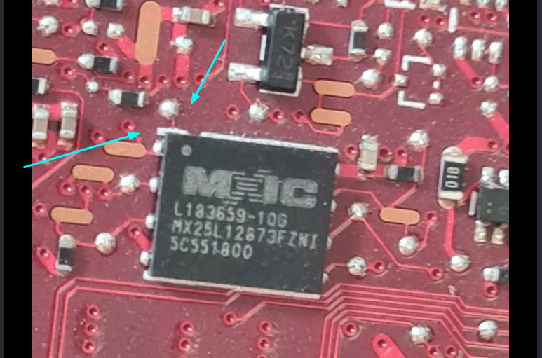
I used the original eprom chip , not the winbond ( that @#!%¨@!¨& said "lets use the original first, if didnt work i ill try with the one you bought)
there is anything i can try, before soldering the other chip?
Which is the best program to use on W25Q128FV ?
I read somewhere that holding ctrl + home with the right bios name on a pendrive would works , but no sucess for me yet
@chadalu - This ^@)_$&@ guy!!! Did he program it with the software and version I mentioned CH341A v1.31(1.4) (CH341AFree)?
If yes, did he choose type 25, size 16MB, then erase first, then blank check, then open BIOS file then write, then verify? << If he did not do this, that may be part of the issue, it should be working if he did all this with correct software.
If it continues to fail, try one of these instead, since most results with this chip ID I’ve seen from users, or my own testing, were NOT in the WSON package >> ASProgrammer 1.4 or 1.41, or CH341A v1.1.1.32 (May detect chip as MX25L12805, it’s OK, move forward)
I tested this chip myself with but in DIP8 package, with CH341A v1.31(1.4) (CH341AFree, and with ASProgrammer 1.40 or 1.41, images shown of all processes OK for both at thread below
[GUIDE] The Beginners Guide to Using a CH341A SPI Programmer/Flasher (With Pictures!) (2)
To write to W25Q128FV use Colibri (included below) or ASProgrammer 1.41, both included below. I think colibri has been confirmed working the most
http://s000.tinyupload.com/index.php?fil…213094641136166
If nothing is working, get that SOIC8 chip on there, then we can fix it while you are at home. I will make you near 100% stock BIOS to get you going, then we’ll sort out the rest with software flashing.
It’s possible there is a ME FW issue causing the result you see now, if it was messed up in the dump you sent me, and then carried over into the clean Updated ME I put in.
We’ll have to try some other known working ME Dump from this same model to sort that out as a possible cause too, if this continues to happen.
Here, use this BIOS no matter what you do moving forward, I forgot to unlock the FD in the previous BIOS I sent you, this only helps with later software flashing of certain regions, nothing to do about fixing things.
https://ufile.io/g941r2ho
I used my old notebook to flash de eprom, i take it there and did as you said using the CH341A v1.31(1.4) (CH341AFree).
0- Selected chip size
1- Read eprom
2- Erase
3- verify
4- flash
5- verify after flash and got a mensage saing SAME CHUNK,( or something like that after flash)
Tomorrow i will get the soic8 on the board and it ill be easier to work this thing out!
Select chip type is missing from your above list, did you choose 25? It should say “chipand buffer same” as shown in my testing image linked above
Also, read eeprom is not a step we do here  Here is step by step you should do for write to chip >>
1. Select 25 and chip size, and or you can try detect
2. Erase chip
3. Blank check
4. Open BIOS file you want to write
5. Write
6. Verify
Yes, once you get the SOIC8 chip on there, we’ll sort it out
Yeah, that what i did,
Sorry i forget to write that i opened the bios file
just after number 1
1 - 25 was selected already when i open the program so i just have to select the chip size!
1,5 - open the bios file you sent to me
and that is the message "chipand buffer same" ( I knew there is the SAME word on it!!!)
I just programmed a SOIC8, here is the log of colibri, I should be back in 2 or 3 hours with the results
We needed to bend the chip legs so it can fit on wson solder pads
With the last flash i did above, not a single signal of life, not leds, monitor or anything turning on
when i press power button nothing happens, nothing at all
the solder looks fine on chip i ill atach some pics
https://imgur.com/a/pwDAGT3
Since the legs are bended, it is hard as hell ataching clip to it, im cutting some plastic of the clip and tryng to read the chip
Update -
1- i think the solder went bad at some point, i reassembled the notebook 2 times , just to be sure that everything is connected, looks like there is no eprom chip at all, even the charging led wont go on.
2- man, i almost eat the chip with the clip, and cant make it detect it,it looks perfect conected all 8 legs, but it just wont find anything 
3- Now , i have to wait until monday to solder other chip (for my luck i bought a pack of 5) if i cant make it work again, i ill go back to the good and old wson boy
4- there is any other possibility of dump that i can use? if i cant make work with that one you sent to me yesterday, Would be nice to had other desesperated options (plan B) ready.
5- i became friend of the guy who is make this soldering, he is not being a bitch anymore
@chadalu - BIOS file should not be opened just after step #1, it must be done when I mentioned, otherwise you can mess up verification, that’s why I made specific outlined steps Do it that way only
Chip legs should not have needed bent at all! It’s this same )P*(^$()@^&% guy again isn’t it? 
Ohh, looking at the images, I guess this is more Asus fault, they did not put a normal SOIC8/WSON connection area there like you’d usually have that would fit either without issue.
This is not “Fine” that is kind of sloppy soldering job, but at least he cleaned up afterwards! If he would have looked at it with a loupe or magnifying glass when he was done he would see it may not all be connected, and some cold solder joints etc.
And it looks like he’s possibly damaged the chip too, can’t tell for sure, but it’s damaged, deep gouges and scratches into the chip body.
Also, in second image, looks like he possibly damaged the board traces on the PCB from BIOS too, two traces look scratched, I can’t tell if cut through trace or not 

I’m talking about the two ones on left side, and those same two legs do not look soldered in very well either, so this may be a point of no contact, thus no power on.
Have him reflow those two legs only, possibly third too on this side, and see if it helps, this may be the only issue, unless those traces are cut through where it’s scratched/gouged on the board PCB
And then also first leg on left side of first image, may be cold solder joint, reflow this too.
For SOIC8 clip, you may need power cable, and or main battery, or both, or only one or other, connected, before you can detect chip.
And yes, sometimes clip is a pain, it may take you many times reclamping before it’s perfect, keep trying, but wait until he reflows that solder otherwise you are wasting your time (since you know the chip is already programmed)
If you have to, yes, go back to WSON, if so, use this BIOS, this will be 100% square one (hopefully your ME FW is not corrupted in the first dump you made, I did not touch it in this BIOS, only unlocked FD and put back your original BIOS region)
This BIOS CANNOT Be used with W128Q128FV chip - http://s000.tinyupload.com/index.php?fil…102789566079162
You do not need other dumps, the BIOS I sent you previously, and the follow-up should work, once chip is on there properly
Good to hear this guy is more friendly to now! Hopefully he is not charging you an arm & a leg to do this work, since if you’ve been watching him you can see it’s very easy to do
Do you have a good image of the board, not cropped off like your first image linked in this thread, but showing that same area before you did anything, so I can see that chip/area?
This concerns me, and I wanted to see if it was maybe there before, or what it looks like in another image, in case it’s hair or dust etc (or possibly scratch or ?)
Yeah, Asus really made my life more dificult in this one! i was there while he is doing this, the region is so small and there is a ton of micro things around!
The Soic8 chip would not fit there without a bend, the pad on the board is wson format!
He is the best person in my city to do this job(Small City Problems), others that i know would have melted my board at this point!
I didnt know about the batery or power cable, since i programed it using the clip without any power, i thought would work at same way using the clip on board
at this point i ill not try anything , i dont want burn anything plugging the baterry or power cord since the solder is no good.
I see the 2 traces that you talking about, i cant tell either if it is damaged or not, since im using my s20 camera to zoom in, and not a real zoom lens, looks like a little damaged, cant tell for sure, i would need a Magnifying glass to be sure
I think i ll go back to wson, im afraid of damaging the board or something else with soic8 soldering, he is not charging me anymore
He wants to see this notebook working, more than i!
about the image you sent , i was scared to hell when read it from my celphone, but it was just my cat hair!
And NO, it dont have acess to my Office!
I dont have any picture of the area before flashing, i take pictures of the entire board , But the most importante part, i dont have any, just the picture of the eproom chip that i have sent to you on first PM
i take other picture of the area , and a best zoomed image of the solder points, thr board pictures are from now
https://imgur.com/a/9srWr8o
Yes, it’s not often chip area like this is constructed into WSON form footprint only, that’s why I initially said no issues with SOIC8 because it’s generally simply swap without having to mess with anything, same in inverse as well
At least now this guy isn’t being such a pain for you
Yes, with chip on the board, sometimes you need battery or main power cable attached, or only one, and sometimes you need them both removed. This all varies from board to board
You wont burn anything, but yeah if connection not good is the issue here, trying to program the chip (which is already properly programmed) wont help anything. Chip should be fine and programmed, so no real need to attach CH341A to it
Before you go back to WSON, have him reflow those 4 legs I mentioned, two look really bad, this may be the only issue.
You have an image of the entire board, you showed me the WSON chip at first post (but image cropped to that chip). This was the image I wanted to see, uncropped. But I guess this is cat hair
Wow, third and fourth image (and last), looks like 3 possibly scratched traces on the board, not just two I mentioned being able to see in those initial images. Hopefully those are not through the coating and breaking the traces! << If so, then even WSON will not work now 
I could try a reflow before going WSON, I ill ask him to take a look to see if there is any real damage on trails,( the worst part is reassemble the notebook, the eprom chip is on the back of the board ! it happens to have a power button onboard, so i dont have to put everything together, but at least 60% of the parts)
i think he has ability to make a jumper if trails is damaged (dont know if is possible, i realllllllllly hope is!!!),
This zoom of s20 camera use some kind of AI that mess with image when you zoom to much,
Using my eye zoom, i think the worst was the botton one that looks like a small hole, the others looks "fine"
That picture was a zoomed image at full resolution, i didnt croped it.
But yes it was my cat hair!i they were sitting in the same location when the picture was taken!!!
I just blowed them, and no more cat hair scratch on mobo!
Here is a new package for WSON ONLY, this includes a 100% Stock Asus BIOS region (minus one volume) + your dumped FD (unlocked) and OG ME, this will not have your system specific details, we’ll fix later!
Second same as above but with clean/UPD ME, both this and the above also have unlocked FD. And, third is the BIOS I posted at #31. And as a final last resort, I’ve also included a 100% untouched known working dump from another user
If it comes to that last resort, and then boots, then we know your original dumped ME FW was bad and carried over into the clean/updated ME FW and all other BIOS I made you.
That, or your original FD was corrupted possibly, or both. I’m asking another user for FD dump below, to have third comparison.
Anyway, this way you have four BIOS to try to boot from on WSON, if you go back to that. Keep in mind, these BIOS will ONLY work on the WSON chip!
http://s000.tinyupload.com/index.php?fil…612440331816375
None of these are unlocked, other than unlocked FD, we’ll redo your menu properly once you’re back up and running
Before going back WSON though, I suggest you have him reflow those 2-3 legs on one side and the one leg on other side, then try again and see if it boots.
During boot up attempts, do not connect HDD/SSD, and put in only one stick of memory in first slot, or at least attempt to boot with only one stick first, then put in second.
This way, if CMOS is retaining anything in any of these non-stock BIOS it will reset things.
Yes, if traces are damaged you can jump past, but if he did damage it during this work, it’s unlikely that he’s steady handed enough to do that kind of re-work without possibly making things worse. Unless he just jumps from leg or pad to the dots and copper pad well past the trace area.
Yeah, I can’t tell from those images, if the protective coating right near the legs is just scratched, or the actual copper trace underneath is scratched too. Those are so fine, that if it’s scratching into the copper trace it’s probably broken the path.
Hard to tell this in person even, unless you put under good light, look with magnification, and or maybe get it wet or put clear flux on it, so you remove the “white-ness” of the scratch itself and can see what’s actually scratched and what’s not.
The image above is 100% scratches, not cat hair, just so we’re clear, that I was talking about two different things there with the above and then what I assume you mean as cat hair on the other area (not BIOS chip location)
@cowpod - Would you mind, dumping your FD and ME from your GL504GW for me with FPT, so I can check something for user here, thanks 
FPTw.exe -desc -d fd.bin
FPTw.exe -me -d me.bin
Fine, just to be clear this is the order i should try first.
1-SQ1FD.bin
2-SQ1FD-STKRGNVol1-6UEFIT-Vol7SH.bin
3-SQ1FD-STKRGNVol1-6UEFIT-Vol7SH-MECUPD.bin
4-noah0105.bin (last resort)
I ill check the traces first, if it is damaged or close to be, i ill give up on soic8, since he used the iron to solder the soic8, more damages are possible!
And yes, the car hair was on the image that you sent on post #33, not the bios area!
should i wait the cowpod bios dump before try anything?
I hope tomorrow i ill bring you good news !
Yes, that order would be best to try You can add this to top of that list too >> OGRegInMEFWUPDVSCCAddFD
If the traces are damaged, it does not matter what kind of chip you use, any damage to trace will affect either chips connection to the rest of the board.
That is not cat hair on image #33, can’t be, especially because it exactly follows the traces, if you think so please show me new images and I will look again but I can already tell you this isn’t cat hair for sure.
That image I posted is from your new images from post #32, after you said you seen cat hair
On image #31 maybe yes, but not #33, that is scratches to the PCB, I can see on all images easily.
No, I only asked cowpod for FD and ME, so I could look at something, in case maybe later we need to try other things.
The BIOS I sent you to put on SOIC8 chip should work on either, so it can really be tested first, then the 4 above if you wanted
If it gets down to noah01015 BIOS and still nothing, then anything cowpod sends me wont matter either, because really if none of the BIOS I made you based on your dump work, and then noah0105’s BIOS does not work, something else is wrong.
Sorry , i mencioned the wrong post, the right one is #31, as you said!
Ok, lets begin @Lost_N_BIOS
The soic8 chip soldering was fine and all the legs were sodered. So i decided to move to WSON.
I flashed the SQ1FD.bin, like the first file you sent to me, it boots on asus splash screen, but remains there, so i cant give any command or enter bios,
So i moved to last Resort (sorry i was late and need to leave, so i skipped the 2 and 3, and i was afraid that the board could suffer any damage by solder and remove the chip 4 times),and the same thing happens as the other files
It first boots flashing all leds colors (it does this show when you flash a bios update), them it reboots, so the leds become red, the splash screen apperas and right after they go all colors again (supposed to stay red and boot).
the funny thing is,if turn off and on again this process repeat again! there is any chance that bios have some write protection that prevents notebook from set it defaults settings and boot? or something like that?
i think the bios is fine, looks like something is preventing it from move foward!
I cant tell what is going on, since i used the last resort, it supposed to boot, maybe it was the bios version? i have a ftp dump of my bios on 305 version! (but dont have chip dump on this one),
The guy says that he can solder 8 thin wires on the pads just after the eprom chip, and make me like a jumper cable, so it ill work like the clip, and i dont have to teardown the notebook every time.
He said if the uses too much hot air on the area, the protective coat of the board will go off, and there is a risk of damaging the trails
I made a video when i turn it on
https://youtu.be/8Dss6JBmGjk
here another pics of the area, looks like no damage on the trails
https://imgur.com/a/tD7tmKi
and the 305 dump
http://www.mediafire.com/file/qbsuvnvqy26c20h/file
@chadalu - The soldering was not “fine” for sure at least 3 legs needed properly reflowed, no matter what that guy said or thought, this should be done
Did you try, remove hard drive and one stick of memory, then try to boot it again, to try and reset CMOS even though BIOS programming should have done that anyway this may help.
Try this, and try remove the CMOS battery and boot once too
It may be that when you change the setting you changed about XTU, this changed something on EC/KBC FW, and that may be the issue. This is on other chip, sometimes you can’t even read/write this chip without doing via KB ribbon cable.
BIOS version does not matter in this case, we’re using the one you were on so it would match EC/KBC FW if that were to be any issue.
Dump the Winbond W25Q80EW with 1.8v adapter, and send to me, I can check it to see if anything looks corrupted, and see if this is the EC/KBC FW chip or not (may be vBIOS, we have to see)
The image link above does not load any images Can you please re-up, or put in zip would be better, thanks
The two files you skipped were most likely to be bootable, vs the first one. Unsure about last one, since it’s another users, but it should boot too I assumed
The two you skipped though, were 100% stock BIOS region, but yes, it’s not good to continually remove/reapply this chip, that’s why I suggested you put on the SOIC8 to begin with (Should really leave, once properly soldered in).
Yes, maybe wires soldered in place would be helpful for you, but you’d need an adapter on the end that would fit either SOIC8 or WSON, or DIP8 and you purchase a DIP8 chip.