Hello, i want to mod my Bios (E1782IMS.122),
with afudos i get the checksum error, mostly becauso of the oem Protection, how can i unblock my bios to enable flashing?
thanks for your help
luki
@luki508 - For your mod BIOS, did you try flashing from within the BIOS with BIOS on USB, but mod BIOS renamed to exact name as the stock BIOS including extension too?
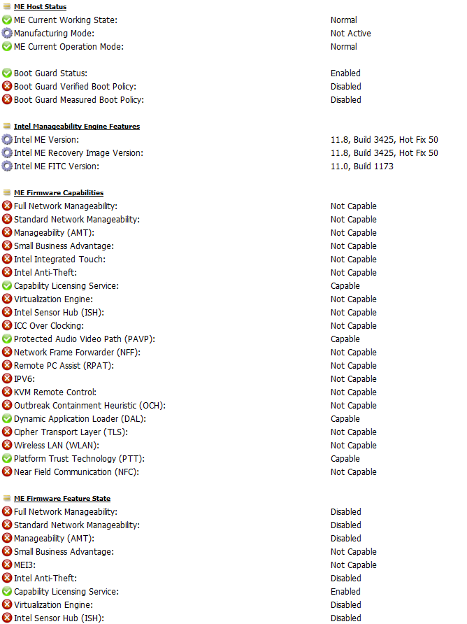
If yes, and no luck still, please check your BIOS Main page and see if you can find ME FW version, if not download HWINFO64 and check with it on large window, on left expand motherboard section then go to ME and find ME firmware version.
Then download matching Intel ME System Tools package from this thread in section “C” Inside you will find Flash Programming Tools folder, and inside that a windows or Win/Win32 folder.
Select the “Win or Win32 etc” folder, hold shift and press right click, choose open command window here, then enter the following command and zip and attach the output file
FPTw.exe -bios -d biosreg.bin
On a copy of this file, you do your modifications that you want flashed. You don’t need to send me that modified, just the stock output is fine, but this is the file you need to redo your mods on again, then we will reflash it once I tell you how to unlock BIOS lock
Intel Management Engine: Drivers, Firmware & System Tools
i think you mean this thread,
i have
Intel ME Version: 11.8, Build 3425, Hot Fix 50
Intel ME Recovery Image Version: 11.8, Build 3425, Hot Fix 50
Intel ME FITC Version: 11.0, Build 1173
but in this threat there isn`t a version for Build 11 or do you mean this?:
Intel CSME System Tools v11 r20 - (2019-01-23)
Thank you

@luki508 - Sorry, yes, I forgot to add link to that thread! Did you try renaming mod BIOS to exact name of stock BIOS including extension and no luck flashing from within BIOS?
If not, then we’ll have to do FPT way. Yes, download V11 ME System Tools Package, then run the command I gave you above, upload the created file for me to look at, and then wait I’ll send back to you with a setting unlocked, then you will do your mod again on the file I send you back.
Then I will help you unlock the setting I unlocked in your dump, but on your current BIOS, so you can then reflash the final re-modified biosreg.bin dump we both edit.
so this is my output file ( its in a zip, because bin files arent allowed), is there a tool with i can modify this biosreg.bin file?
i only tried to flash the file generated AMIBCP, but this file is .rom file and if i flash it within the bios it says wrong file format.
thank you for your help
edit
can i use amibcp to mod also .bin files?
biosreg.zip (3 MB)
if i try to rename the biosreg.bin to the original name E1782IMS.122 the bios says warning, wrong image format
@luki508 - biosreg.bin? I thought you modified the stock BIOS and was trying to flash that, not biosreg.bin? You’re confusing things I said together that shouldn’t be mixed up, please re-read carefully everything I mentioned.
biosreg.bin and FPT have nothing to do with renaming your originally modified BIOS file. I mentioned renaming, as in your main issue was you couldn’t flash your modified BIOS file, before I mentioned anything about FPT or biosreg.bin.
And I said to wait to flash anything with FPT until I checked it, because of what you need to do below. Please slow down, be VERY careful with FPT, you will brick your board instantly if used improperly!
It’s very likely half or all the changes you made in AMIBCP wont apply anyway, so there is no rush
What I said first was, your originally modified BIOS, I assumed was the stock BIOS you modified with AMIBCP… Correct? If yes, rename that to stock name and flash via USB within the BIOS.
If that does not work, which it usually does, stop there, none of this statement applies to anything else, and none of the FPT stuff applies to this file anymore either.
bin/rom = same/same rename anytime to either one, as desired or needed.
biosreg.bin, from FPT backup you made, posted in post #5. That you can now modify with AMIBCP, this file you cannot flash with BIOS built in flash tool, only FPT, and that can only be done after you do the following to disable "BIOS Lock"
Follow this guide, starting at step #6, you can skip steps #1-5 because I will give your variable below - [GUIDE] Grub Fix Intel FPT Error 368 - BIOS Lock Asus/Other Mod BIOS Flash
BIOS Lock variable >> 0x5AE
Rename your .efi file to >> Shell.efi
So at grub prompt you will type the following >> setup_var 0x5AE 0x0
Then reboot, and you can now flash your modified biosreg.bin file using FPT and this command (stop if you see any error, show me an image) >> FPTw.exe -bios -f modbiosreg.bin
change name of “modbiosreg.bin” in the command above to whatever you named your modified biosreg.bin file, or name it as you see above.
I can’t boot into efi shell… The option isn’t in my bios
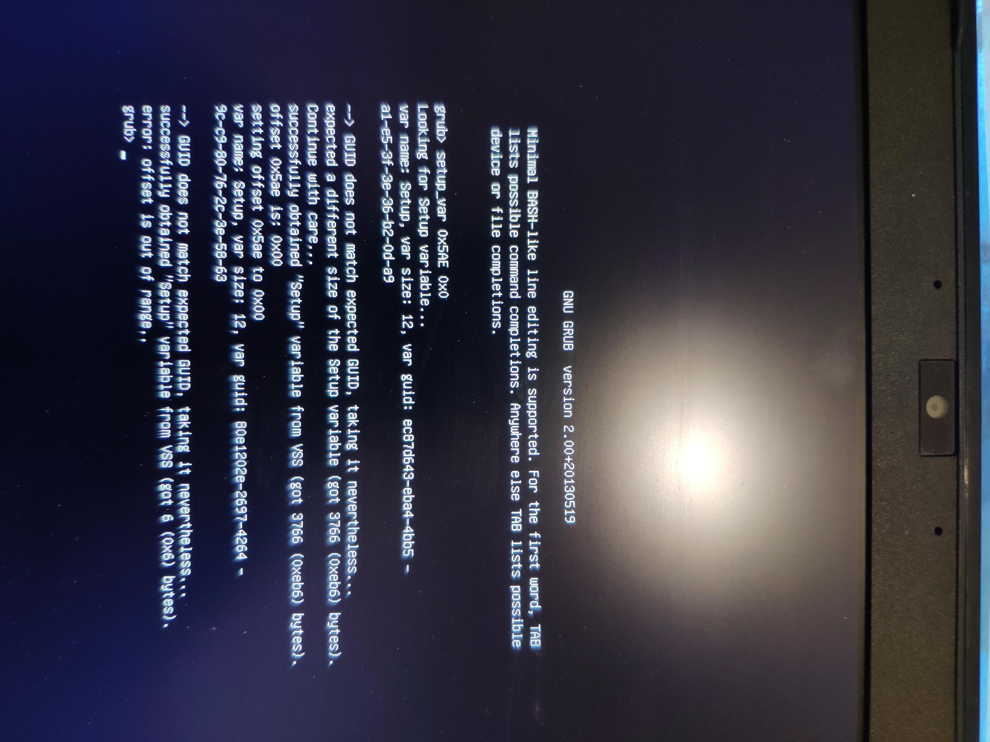
Ok got into efi with your post about how to boot into grub without efi setting in bios… But now in grub i get this message:
Forgot what i said… I now finally flashed the new bios… But no new settings appear in my bios…
Ok sry for to many posts… I now finally made it… The new bios settings appear!
thank you so much
Can i deactivate the bios lock permanently?
And can i lock the cpu on all cores to 3.6 ghz?
@luki508 - Please edit your post to add new info, thanks
You should be able boot to Shell.efi I got that out of your BIOS exit page “Launch EFI Shell from filesystem device” But, maybe it’s hidden from you too?
BIOS Lock can be disabled in BIOS settings, just make that section visible to you. It’s disabled now since you disabled it, but any time you reflash stock or mod BIOS, you need to disable it again first before you reflash.
That can be done by editing the setup module via IFR/Hex, or within AMIBCP. In AMIBCP, it’s in the hidden advanced section at >> Advanced >> PCH-IO Configuration >> BIOS Security Configuration
Yes, you can set default 3.6 at OC >> Adjust CPU Ratio, and per core settings are at hidden advanced >> CPU Config
yeah but my cpu 6700hq can´t push all cores to 3.6 ghz
You can only set as much as Intel spec allow you to set then, sorry for any confusion I didn’t check CPU and only replied about what you asked.
Do you want me to unlock your BIOS for you? If yes, please zip up a package of one single image of each main BIOS pages so I can see what all you see on stock BIOS, just main pages no submenus or deep in settings (Main, Advanced, Chipset, OC, Security, Boot, Save and exit etc)
What didn’t unlock for you in your AMIBCP mod that you still want enabled? not much in there, except in advanced menu. Also, put your mod BIOS in the images zip, so I can see what you did in AMIBCP for the settings you want, that didn’t work
i already unlocked most of the extra options, but i have not recived any extra performance out of it
modbiosreg.zip (3 MB)
@luki508 - What did you enable with AMIBCP, that didn’t show up in BIOS though? Chipset is empty, nothing to enable there 
i enabled all oc options and all chipset options, all show up. i haven’t unlocked cache options because idk how to work with it
OK, I thought you said you tried to enable some stuff but it didn’t work/didn’t show up, so I was going to look at figuring that out for you.
There is no chipset options, so nothing to enable there  At least not with AMIBCP, however, chipset can be enabled via IFR/Hex edit though, did you do that already (I didn’t check)? There’s a good stack of settings there, that aren’t in the ADV section
Form: Chipset, FormId: 0x2713 {01 86 13 27 1F 00}
0x3D49D End Form {29 02}
0x3D49F Form: SB Porting Configuration, FormId: 0x2726 {01 86 26 27 77 02}
0x3D4A5 Subtitle: Statement.Prompt: SB Porting Configuration, Flags: 0x0 {02 87 79 02 00 00 00}
0x3D4AC End {29 02}
0x3D4AE Subtitle: Statement.Prompt: , Flags: 0x0 {02 87 02 00 00 00 00}
0x3D4B5 End {29 02}
0x3D4B7 Suppress If {0A 82}
0x3D4B9 QuestionId: 0xA6F equals value 0x1 {12 06 6F 0A 01 00}
0x3D4BF Gray Out If {19 82}
0x3D4C1 QuestionId: 0xA51 equals value 0x1 {12 06 51 0A 01 00}
0x3D4C7 Suppress If {0A 82}
0x3D4C9 QuestionId: 0x18 equals value 0x1 {12 86 18 00 01 00}
0x3D4CF Not {17 02}
0x3D4D1 QuestionId: 0x95A equals value 0x0 {12 06 5A 09 00 00}
0x3D4D7 Or {16 02}
0x3D4D9 End {29 02}
0x3D4DB One Of: SATA RAID ROM, VarStoreInfo (VarOffset/VarName): 0x33, VarStore: 0x1, QuestionId: 0x9F9, Size: 1, Min: 0x0, Max 0x2, Step: 0x0 {05 91 7C 02 7D 02 F9 09 01 00 33 00 10 10 00 02 00}
0x3D4EC One Of Option: Legacy ROM, Value (8 bit): 0x0 {09 07 7E 02 00 00 00}
0x3D4F3 One Of Option: UEFI Driver, Value (8 bit): 0x1 {09 07 7F 02 00 00 01}
0x3D4FA One Of Option: Both, Value (8 bit): 0x2 (default) {09 07 80 02 30 00 02}
0x3D501 End One Of {29 02}
0x3D503 End If {29 02}
0x3D505 End If {29 02}
0x3D507 End If {29 02}
0x3D509 Suppress If {0A 82}
0x3D50B QuestionId: 0xA6F equals value 0x0 {12 06 6F 0A 00 00}
0x3D511 Gray Out If {19 82}
0x3D513 QuestionId: 0xA51 equals value 0x1 {12 06 51 0A 01 00}
0x3D519 Suppress If {0A 82}
0x3D51B QuestionId: 0x95A equals value 0x0 {12 06 5A 09 00 00}
0x3D521 One Of: SATA RAID ROM, VarStoreInfo (VarOffset/VarName): 0x33, VarStore: 0x1, QuestionId: 0x9FA, Size: 1, Min: 0x0, Max 0x2, Step: 0x0 {05 91 7C 02 7D 02 FA 09 01 00 33 00 10 10 00 02 00}
0x3D532 One Of Option: Legacy ROM, Value (8 bit): 0x0 {09 07 7E 02 00 00 00}
0x3D539 One Of Option: UEFI Driver, Value (8 bit): 0x1 {09 07 7F 02 00 00 01}
0x3D540 One Of Option: Both, Value (8 bit): 0x2 (default) {09 07 80 02 30 00 02}
0x3D547 End One Of {29 02}
0x3D549 End If {29 02}
0x3D54B End If {29 02}
0x3D54D End If {29 02}
0x3D54F End Form {29 02}
0x3D551 Form: NB Porting Configuration, FormId: 0x2774 {01 86 74 27 76 02}
0x3D557 End Form {29 02}
0x3D559 Form: OC, FormId: 0x2714 {01 86 14 27 78 12}
0x3D55F Subtitle: Statement.Prompt: Overclocking can be harmful to your system, please use at your own risk., Flags: 0x0 {02 87 7A 12 00 00 00}
0x3D566 End {29 02}
0x3D568 Subtitle: Statement.Prompt: , Flags: 0x0 {02 87 02 00 00 00 00}
0x3D56F End {29 02}
0x3D571 Subtitle: Statement.Prompt: CPU, Flags: 0x0 {02 87 7B 12 00 00 00}
0x3D578 End {29 02}
0x3D57A Gray Out If {19 82}
0x3D57C QuestionId: 0xA51 equals value 0x1 {12 06 51 0A 01 00}
0x3D582 One Of: Full Fan Speed, VarStoreInfo (VarOffset/VarName): 0x41, VarStore: 0x1, QuestionId: 0x9FB, Size: 1, Min: 0x0, Max 0x1, Step: 0x0 {05 91 AF 12 B0 12 FB 09 01 00 41 00 10 10 00 01 00}
0x3D593 One Of Option: Disabled, Value (8 bit): 0x0 (default) {09 07 04 00 30 00 00}
0x3D59A One Of Option: Enabled, Value (8 bit): 0x1 {09 07 03 00 00 00 01}
0x3D5A1 End One Of {29 02}
0x3D5A3 End If {29 02}
0x3D5A5 Subtitle: Statement.Prompt: , Flags: 0x0 {02 87 02 00 00 00 00}
0x3D5AC End {29 02}
0x3D5AE Gray Out If {19 82}
0x3D5B0 QuestionId: 0xA51 equals value 0x1 {12 06 51 0A 01 00}
0x3D5B6 Numeric: Adjust CPU Ratio, VarStoreInfo (VarOffset/VarName): 0x5C, VarStore: 0x1, QuestionId: 0x272D, Size: 1, Min: 0x0, Max 0x32, Step: 0x1 {07 91 7C 12 7D 12 2D 27 01 00 5C 00 14 10 00 32 01}
0x3D5C7 Default: DefaultId: 0x0, Value (8 bit): 0x0 {5B 06 00 00 00 00}
0x3D5CD End {29 02}
0x3D5CF End If {29 02}
0x3D5D1 Text: Statement.Prompt: Adjusted CPU Frequency, TextTwo: N/A {03 08 7E 12 80 12 7F 12}
0x3D5D9 Gray Out If {19 82}
0x3D5DB QuestionId: 0xA51 equals value 0x1 {12 06 51 0A 01 00}
0x3D5E1 Numeric: Adjust Ring Ratio, VarStoreInfo (VarOffset/VarName): 0x65, VarStore: 0x1, QuestionId: 0x9FC, Size: 1, Min: 0x0, Max 0x32, Step: 0x1 {07 91 81 12 82 12 FC 09 01 00 65 00 10 10 00 32 01}
0x3D5F2 Default: DefaultId: 0x0, Value (8 bit): 0x0 {5B 06 00 00 00 00}
0x3D5F8 End {29 02}
0x3D5FA End If {29 02}
0x3D5FC Gray Out If {19 82}
0x3D5FE QuestionId: 0xA51 equals value 0x1 {12 06 51 0A 01 00}
0x3D604 Numeric: CPU Core Voltage, VarStoreInfo (VarOffset/VarName): 0x5E, VarStore: 0x1, QuestionId: 0x9FD, Size: 2, Min: 0x0, Max 0x5DC, Step: 0x1 {07 94 85 12 86 12 FD 09 01 00 5E 00 10 11 00 00 DC 05 01 00}
0x3D618 Default: DefaultId: 0x0, Value (16 bit): 0x0 {5B 07 00 00 01 00 00}
0x3D61F End {29 02}
0x3D621 End If {29 02}
0x3D623 Gray Out If {19 82}
0x3D625 QuestionId: 0xA51 equals value 0x1 {12 06 51 0A 01 00}
0x3D62B Numeric: CPU Core Voltage Offset, VarStoreInfo (VarOffset/VarName): 0x60, VarStore: 0x1, QuestionId: 0x9FE, Size: 2, Min: 0x0, Max 0xFA, Step: 0x1 {07 94 89 12 8A 12 FE 09 01 00 60 00 10 11 00 00 FA 00 01 00}
0x3D63F Default: DefaultId: 0x0, Value (16 bit): 0x0 {5B 07 00 00 01 00 00}
0x3D646 End {29 02}
0x3D648 End If {29 02}
0x3D64A Gray Out If {19 82}
0x3D64C QuestionId: 0xA51 equals value 0x1 {12 06 51 0A 01 00}
0x3D652 Numeric: CPU RING Voltage, VarStoreInfo (VarOffset/VarName): 0x67, VarStore: 0x1, QuestionId: 0x9FF, Size: 2, Min: 0x0, Max 0x5DC, Step: 0x1 {07 94 87 12 88 12 FF 09 01 00 67 00 10 11 00 00 DC 05 01 00}
0x3D666 Default: DefaultId: 0x0, Value (16 bit): 0x0 {5B 07 00 00 01 00 00}
0x3D66D End {29 02}
0x3D66F End If {29 02}
0x3D671 Subtitle: Statement.Prompt: BCLK, Flags: 0x0 {02 87 99 12 00 00 00}
0x3D678 End {29 02}
0x3D67A Gray Out If {19 82}
0x3D67C QuestionId: 0xA51 equals value 0x1 {12 06 51 0A 01 00}
0x3D682 Numeric: Clock Frequency, VarStoreInfo (VarOffset/VarName): 0x2, VarStore: 0x1A, QuestionId: 0x272E, Size: 2, Min: 0x2710, Max 0xFFFF, Step: 0xA {07 94 B5 02 B7 02 2E 27 1A 00 02 00 14 11 10 27 FF FF 0A 00}
0x3D696 Default: DefaultId: 0x0, Value (16 bit): 0x2710 {5B 07 00 00 01 10 27}
0x3D69D End {29 02}
0x3D69F End If {29 02}
0x3D6A1 Subtitle: Statement.Prompt: , Flags: 0x0 {02 87 02 00 00 00 00}
0x3D6A8 End {29 02}
0x3D6AA Subtitle: Statement.Prompt: CPU Core IccMax, Flags: 0x0 {02 87 9A 12 00 00 00}
0x3D6B1 End {29 02}
0x3D6B3 Gray Out If {19 82}
0x3D6B5 QuestionId: 0xA51 equals value 0x1 {12 06 51 0A 01 00}
0x3D6BB Numeric: VR Current Limit, VarStoreInfo (VarOffset/VarName): 0x246, VarStore: 0x1, QuestionId: 0xA00, Size: 2, Min: 0x0, Max 0x3FE, Step: 0x1 {07 94 12 02 13 02 00 0A 01 00 46 02 10 11 00 00 FE 03 01 00}
0x3D6CF Default: DefaultId: 0x0, Value (16 bit): 0x0 {5B 07 00 00 01 00 00}
0x3D6D6 Default: DefaultId: 0x1, Value (16 bit): 0x0 {5B 07 01 00 01 00 00}
0x3D6DD End {29 02}
0x3D6DF End If {29 02}
0x3D6E1 Subtitle: Statement.Prompt: Turbo Boost Power Max, Flags: 0x0 {02 87 9B 12 00 00 00}
0x3D6E8 End {29 02}
0x3D6EA Gray Out If {19 82}
0x3D6EC QuestionId: 0xA51 equals value 0x1 {12 06 51 0A 01 00}
0x3D6F2 Numeric: Power Limit 1, VarStoreInfo (VarOffset/VarName): 0x38, VarStore: 0x1, QuestionId: 0xA01, Size: 2, Min: 0x0, Max 0x1F4, Step: 0x1 {07 94 DB 00 DC 00 01 0A 01 00 38 00 10 11 00 00 F4 01 01 00}
0x3D706 Default: DefaultId: 0x0, Value (16 bit): 0xC8 {5B 07 00 00 01 C8 00}
0x3D70D End {29 02}
0x3D70F End If {29 02}
0x3D711 Subtitle: Statement.Prompt: Turbo Boost Short Power Max, Flags: 0x0 {02 87 9C 12 00 00 00}
0x3D718 End {29 02}
0x3D71A Gray Out If {19 82}
0x3D71C QuestionId: 0xA51 equals value 0x1 {12 06 51 0A 01 00}
0x3D722 Numeric: Power Limit 2, VarStoreInfo (VarOffset/VarName): 0x3A, VarStore: 0x1, QuestionId: 0xA02, Size: 2, Min: 0x0, Max 0x1F4, Step: 0x1 {07 94 E1 00 E2 00 02 0A 01 00 3A 00 10 11 00 00 F4 01 01 00}
0x3D736 Default: DefaultId: 0x0, Value (16 bit): 0xC8 {5B 07 00 00 01 C8 00}
0x3D73D End {29 02}
0x3D73F End If {29 02}
0x3D741 Subtitle: Statement.Prompt: , Flags: 0x0 {02 87 02 00 00 00 00}
0x3D748 End {29 02}
0x3D74A Gray Out If {19 82}
0x3D74C QuestionId: 0xA51 equals value 0x1 {12 06 51 0A 01 00}
0x3D752 Ref: User Profile, VarStoreInfo (VarOffset/VarName): 0xFFFF, VarStore: 0x0, QuestionId: 0xA03, FormId: 0x272B {0F 0F 8B 12 8C 12 03 0A 00 00 FF FF 00 2B 27}
0x3D761 End If {29 02}
0x3D763 Subtitle: Statement.Prompt: , Flags: 0x0 {02 87 02 00 00 00 00}
0x3D76A End {29 02}
0x3D76C Subtitle: Statement.Prompt: Memory Module, Flags: 0x0 {02 87 9D 12 00 00 00}
0x3D773 End {29 02}
0x3D775 Gray Out If {19 82}
0x3D777 QuestionId: 0xA51 equals value 0x1 {12 06 51 0A 01 00}
0x3D77D One Of: DRAM Profile, VarStoreInfo (VarOffset/VarName): 0x4CB, VarStore: 0x1, QuestionId: 0x273A, Size: 1, Min: 0x0, Max 0x3, Step: 0x0 {05 91 43 03 44 03 3A 27 01 00 CB 04 14 10 00 03 00}
0x3D78E One Of Option: Default DIMM profile, Value (8 bit): 0x0 (default) {09 07 45 03 30 00 00}
0x3D795 One Of Option: Custom profile, Value (8 bit): 0x1 {09 07 48 03 00 00 01}
0x3D79C One Of Option: XMP Profile 1, Value (8 bit): 0x2 {09 07 46 03 00 00 02}
0x3D7A3 One Of Option: XMP Profile 2, Value (8 bit): 0x3 {09 07 47 03 00 00 03}
0x3D7AA End One Of {29 02}
0x3D7AC End If {29 02}
0x3D7AE Gray Out If {19 82}
0x3D7B0 QuestionId: 0x273A equals value 0x1 {12 86 3A 27 01 00}
0x3D7B6 Not {17 02}
0x3D7B8 End {29 02}
0x3D7BA One Of: DRAM Reference Clock (MHz), VarStoreInfo (VarOffset/VarName): 0x3CC, VarStore: 0x1, QuestionId: 0xA04, Size: 1, Min: 0x0, Max 0x2, Step: 0x0 {05 91 39 03 3A 03 04 0A 01 00 CC 03 10 10 00 02 00}
0x3D7CB One Of Option: Auto, Value (8 bit): 0x0 {09 07 60 06 00 00 00}
0x3D7D2 One Of Option: 133, Value (8 bit): 0x1 (default) {09 07 3C 03 30 00 01}
0x3D7D9 One Of Option: 100, Value (8 bit): 0x2 {09 07 3B 03 00 00 02}
0x3D7E0 End One Of {29 02}
0x3D7E2 Text: Statement.Prompt: DRAM Frequency, TextTwo: N/A {03 08 9E 12 9F 12 85 06}
0x3D7EA One Of: QCLK ODD Ratio, VarStoreInfo (VarOffset/VarName): 0x3CF, VarStore: 0x1, QuestionId: 0xA05, Size: 1, Min: 0x0, Max 0x1, Step: 0x0 {05 91 3F 03 40 03 05 0A 01 00 CF 03 10 10 00 01 00}
0x3D7FB One Of Option: Disabled, Value (8 bit): 0x0 (default) {09 07 04 00 30 00 00}
0x3D802 One Of Option: Enabled, Value (8 bit): 0x1 {09 07 03 00 00 00 01}
0x3D809 End One Of {29 02}
0x3D80B Subtitle: Statement.Prompt: , Flags: 0x0 {02 87 02 00 00 00 00}
0x3D812 End {29 02}
0x3D814 Text: Statement.Prompt: Main Timing Configuration, TextTwo: {03 08 A2 12 02 00 6D 00}
0x3D81C Numeric: Command Rate (CR), VarStoreInfo (VarOffset/VarName): 0x3DF, VarStore: 0x1, QuestionId: 0x2745, Size: 1, Min: 0x0, Max 0x2, Step: 0x1 {07 91 5F 03 60 03 45 27 01 00 DF 03 14 10 00 02 01}
0x3D82D Default: DefaultId: 0x0, Value (8 bit): 0x0 {5B 06 00 00 00 00}
0x3D833 End {29 02}
0x3D835 Numeric: tCL, VarStoreInfo (VarOffset/VarName): 0x3D0, VarStore: 0x1, QuestionId: 0x273B, Size: 1, Min: 0x0, Max 0x1F, Step: 0x1 {07 91 49 03 4A 03 3B 27 01 00 D0 03 14 10 00 1F 01}
0x3D846 Default: DefaultId: 0x0, Value (8 bit): 0x0 {5B 06 00 00 00 00}
0x3D84C End {29 02}
0x3D84E Numeric: tRCD/tRP, VarStoreInfo (VarOffset/VarName): 0x3D6, VarStore: 0x1, QuestionId: 0x273C, Size: 1, Min: 0x0, Max 0x3F, Step: 0x1 {07 91 4B 03 4C 03 3C 27 01 00 D6 03 14 10 00 3F 01}
0x3D85F Default: DefaultId: 0x0, Value (8 bit): 0x0 {5B 06 00 00 00 00}
0x3D865 End {29 02}
0x3D867 Numeric: tRAS, VarStoreInfo (VarOffset/VarName): 0x3D4, VarStore: 0x1, QuestionId: 0x273D, Size: 2, Min: 0x0, Max 0x40, Step: 0x1 {07 94 4D 03 4E 03 3D 27 01 00 D4 03 14 11 00 00 40 00 01 00}
0x3D87B Default: DefaultId: 0x0, Value (16 bit): 0x0 {5B 07 00 00 01 00 00}
0x3D882 End {29 02}
0x3D884 Numeric: tRFC, VarStoreInfo (VarOffset/VarName): 0x3D9, VarStore: 0x1, QuestionId: 0x2741, Size: 2, Min: 0x0, Max 0x3FF, Step: 0x1 {07 94 55 03 56 03 41 27 01 00 D9 03 14 11 00 00 FF 03 01 00}
0x3D898 Default: DefaultId: 0x0, Value (16 bit): 0x0 {5B 07 00 00 01 00 00}
0x3D89F End {29 02}
0x3D8A1 Numeric: tREFI, VarStoreInfo (VarOffset/VarName): 0x3D7, VarStore: 0x1, QuestionId: 0x2740, Size: 2, Min: 0x0, Max 0xFFFF, Step: 0x1 {07 94 53 03 54 03 40 27 01 00 D7 03 14 11 00 00 FF FF 01 00}
0x3D8B5 Default: DefaultId: 0x0, Value (16 bit): 0x0 {5B 07 00 00 01 00 00}
0x3D8BC End {29 02}
0x3D8BE One Of: tWR, VarStoreInfo (VarOffset/VarName): 0x3DD, VarStore: 0x1, QuestionId: 0xA06, Size: 1, Min: 0x0, Max 0x18, Step: 0x0 {05 91 5B 03 5C 03 06 0A 01 00 DD 03 10 10 00 18 00}
0x3D8CF One Of Option: Auto, Value (8 bit): 0x0 (default) {09 07 60 06 30 00 00}
0x3D8D6 One Of Option: 5, Value (8 bit): 0x5 {09 07 1E 03 00 00 05}
0x3D8DD One Of Option: 6, Value (8 bit): 0x6 {09 07 1F 03 00 00 06}
0x3D8E4 One Of Option: 7, Value (8 bit): 0x7 {09 07 20 03 00 00 07}
0x3D8EB One Of Option: 8, Value (8 bit): 0x8 {09 07 21 03 00 00 08}
0x3D8F2 One Of Option: 10, Value (8 bit): 0xA {09 07 23 03 00 00 0A}
0x3D8F9 One Of Option: 12, Value (8 bit): 0xC {09 07 25 03 00 00 0C}
0x3D900 One Of Option: 14, Value (8 bit): 0xE {09 07 27 03 00 00 0E}
0x3D907 One Of Option: 16, Value (8 bit): 0x10 {09 07 29 03 00 00 10}
0x3D90E One Of Option: 18, Value (8 bit): 0x12 {09 07 2B 03 00 00 12}
0x3D915 One Of Option: 20, Value (8 bit): 0x14 {09 07 2D 03 00 00 14}
0x3D91C One Of Option: 24, Value (8 bit): 0x18 {09 07 31 03 00 00 18}
0x3D923 End One Of {29 02}
0x3D925 Numeric: tWTR, VarStoreInfo (VarOffset/VarName): 0x3DE, VarStore: 0x1, QuestionId: 0x2744, Size: 1, Min: 0x0, Max 0x1C, Step: 0x1 {07 91 5D 03 5E 03 44 27 01 00 DE 03 14 10 00 1C 01}
0x3D936 Default: DefaultId: 0x0, Value (8 bit): 0x0 {5B 06 00 00 00 00}
0x3D93C End {29 02}
0x3D93E Numeric: tRRD, VarStoreInfo (VarOffset/VarName): 0x3DB, VarStore: 0x1, QuestionId: 0x2742, Size: 1, Min: 0x0, Max 0xF, Step: 0x1 {07 91 57 03 58 03 42 27 01 00 DB 03 14 10 00 0F 01}
0x3D94F Default: DefaultId: 0x0, Value (8 bit): 0x0 {5B 06 00 00 00 00}
0x3D955 End {29 02}
0x3D957 Numeric: tRTP, VarStoreInfo (VarOffset/VarName): 0x3DC, VarStore: 0x1, QuestionId: 0x2743, Size: 1, Min: 0x0, Max 0xF, Step: 0x1 {07 91 59 03 5A 03 43 27 01 00 DC 03 14 10 00 0F 01}
0x3D968 Default: DefaultId: 0x0, Value (8 bit): 0x0 {5B 06 00 00 00 00}
0x3D96E End {29 02}
0x3D970 Numeric: tFAW, VarStoreInfo (VarOffset/VarName): 0x3D2, VarStore: 0x1, QuestionId: 0x273F, Size: 2, Min: 0x0, Max 0x3F, Step: 0x1 {07 94 51 03 52 03 3F 27 01 00 D2 03 14 11 00 00 3F 00 01 00}
0x3D984 Default: DefaultId: 0x0, Value (16 bit): 0x0 {5B 07 00 00 01 00 00}
0x3D98B End {29 02}
0x3D98D Numeric: tCWL, VarStoreInfo (VarOffset/VarName): 0x3D1, VarStore: 0x1, QuestionId: 0x273E, Size: 1, Min: 0x0, Max 0x14, Step: 0x1 {07 91 4F 03 50 03 3E 27 01 00 D1 03 14 10 00 14 01}
0x3D99E Default: DefaultId: 0x0, Value (8 bit): 0x0 {5B 06 00 00 00 00}
0x3D9A4 End {29 02}
0x3D9A6 End If {29 02}
0x3D9A8 End Form {29 02}