There is Asus P9X79 with two sockets?
Not that I know, I think @3dsmaxer30 uses a Z9 board.
Sorry for confusing. I didn’t start a new thread for my board with c602 chipset. It’s a asus z9ped8 ws with c602 chip and dual socket system
@3dsmaxer30 , I use the same model.
Interesting that the Root Ports of CPU2 (#1) are displayed differently in your HWInfo Screenshot than in mine.
@3dsmaxer30 Bifurcation seems to be working since on the second CPU bus128 port 2a 2b 2c 2d do show up. The problem cannot be an NVME driver since you dont need one for basic function of NVME storage. Windows has a basic NVME driver (which isnt needed for it to show up in HWiNFO.
To be sure I would try to enable x4x4x4x4 bifurcation for both the x16 slots connected to the 2nd CPU, Move the NVME carrier card from the bottom slot incrementaly to the 4th PCIe slot from the top and check every IIO on PCIbus 128 if any NVME drive shows up anywhere every time you move the card.
If that doesnt work maybe the traces on the motherboard to the second CPU are longer and you can to try Extended Synch under Advanced/PCi Subsystem settings/PCi Express Settings to try to make it work. Beware some of these some of the settings her caused my machine not to boot and required a CMOS clear and total cold boot.
If you lack this PCi Subsystem settings/PCi Express Settings menu in bios i can unlock it for you if you provide your current bios.
Good luck.
Hey!
I have an Asus p9x79 pro with modified bios 4801 so I can boot from nvme devices. Before i had a cheap chinese x4 card for 1 ssd
So recently I purchased the asus hyper m.2 x16 v2 card and I immediately noticed an issue. I had two different ssds but for some reason they couldn’t see each other. So I started looking around and found this forum post on how to fix my issue, however I am having difficulty doing the changes required to my bios. I got stuck where I need to find the hexa code 0F 0F 61 08 62 08 05 00 00 00 FF FF 00 1E 04 to change the 46 to a 47. I checked the bios in HxD and nothing, nothing is there. I suppose that is because the board i have has a different bios? How do I do the necessary changes?
Another question I have is what would happen if I flashed the bios of the asus p9x79 deluxe. Not the golden one, the one thats just blue and white/gray? Any kind of response would be immensely helpful. Have a nice day
@AmonRatWR - Somehow, no one has requested P9X79 PRO NVME Bifurcation mod, it’s a miracle!!  So, here is fresh mod
Flash via USB Flashback 
http://s000.tinyupload.com/index.php?fil…230067417655230
1 Like
After a few bsod’s finally managing to make it work. Thank you a lot!
Hi there, thanks for the awesome font of information and experience.
I’m trying to do pcie bifurcation on an ASUS Z9PA-D8 with this setup:
- Proxmox VE
- 2x E2667v2
- 8x 16GB DDR3 1600
- Moded Bios 5602 and enabled the hidden menus for pcie bifurcation on IOH 0 and IOH 1
PCI Slots:
S2(PCIE1 x8 2.0): Empty
S3(PCIE2 x16 3.0): Asus Hyper M.2 x16 V2 with 4 Nvme [x8 when S4 populated]
S4(PCIE3 x8 3.0): Empty
S5(PCIE4 x16 3.0): Intel Eth 4x1Gbit [x8 when S6 populated]
S6(PCIE5 x8 3.0): LSI Raid card
SA(PIKE): Empty
The problem I have is when I set up the bifurcation on the IOU2 to x4x4x4x4 for IOH 0 and IOH 1 and I save the changes, after reboot the speed returns to the x16 like something is overwritting it or not being saved.
lspci is only showing one nvme and not showing any splitted pcie port.
Am I missing something?
Thanks for the help.
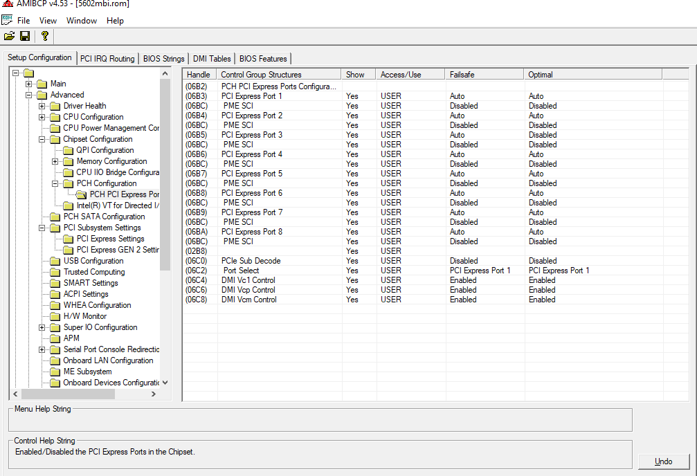
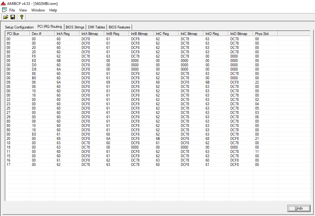
PS: I have only edit the bios with AMIBCP 4.53 converted to ROM and flashed with
@paranoid_android how did you manage to make work your Z9PE-D8-WS with bifurcation, I think is the most similiar motherboard to mine, Z9PA-D8. Can you help me? Thanks
PS2: I uploaded the moded bios
Edit:
Maybe I have to disable PCIE3 here? It shows 8 pcie ports but there are only 5 physical ports and the PIKE
Edit2: dmi decode type 9 info, in effect 6 pcie ports
1
2
3
4
5
6
7
8
9
10
11
12
13
14
15
16
17
18
19
20
21
22
23
24
25
26
27
28
29
30
31
32
33
34
35
36
37
38
39
40
41
42
43
44
45
46
47
48
49
50
51
52
53
54
55
56
57
58
59
60
61
62
63
64
65
66
67
68
69
70
71
72
73
74
75
76
77
78
79
80
81
82
2
3
4
5
6
7
8
9
10
11
12
13
14
15
16
17
18
19
20
21
22
23
24
25
26
27
28
29
30
31
32
33
34
35
36
37
38
39
40
41
42
43
44
45
46
47
48
49
50
51
52
53
54
55
56
57
58
59
60
61
62
63
64
65
66
67
68
69
70
71
72
73
74
75
76
77
78
79
80
81
82
# dmidecode  --type 9
# dmidecode 3.0
Getting SMBIOS data from sysfs.
SMBIOS 2.7 present.

Handle 0x002E, DMI type 9, 17 bytes
System Slot Information
        Designation: PCIE1
        Type: x8 PCI Express x8
        Current Usage: Available
        Length: Short
        ID: 1
        Characteristics:
                3.3 V is provided
                Opening is shared
                PME signal is supported
        Bus Address: 0000:ff:02.2

Handle 0x002F, DMI type 9, 17 bytes
System Slot Information
        Designation: PCIE2
        Type: x16 PCI Express x16
        Current Usage: In Use
        Length: Short
        ID: 2
        Characteristics:
                3.3 V is provided
                Opening is shared
                PME signal is supported
        Bus Address: 0000:03:02.0

Handle 0x0030, DMI type 9, 17 bytes
System Slot Information
        Designation: PCIE3
        Type: x8 PCI Express x8
        Current Usage: Available
        Length: Short
        ID: 3
        Characteristics:
                3.3 V is provided
                Opening is shared
                PME signal is supported
        Bus Address: 0000:ff:03.2

Handle 0x0031, DMI type 9, 17 bytes
System Slot Information
        Designation: PCIE4
        Type: x16 PCI Express x16
        Current Usage: In Use
        Length: Short
        ID: 4
        Characteristics:
                3.3 V is provided
                Opening is shared
                PME signal is supported
        Bus Address: 0000:04:03.0

Handle 0x0032, DMI type 9, 17 bytes
System Slot Information
        Designation: PCIE5
        Type: x4 PCI Express x8
        Current Usage: In Use
        Length: Short
        ID: 6
        Characteristics:
                3.3 V is provided
                Opening is shared
                PME signal is supported
        Bus Address: 0000:06:1c.0

Handle 0x0033, DMI type 9, 17 bytes
System Slot Information
        Designation: PIKE1
        Type: x4 PCI Express x4
        Current Usage: Available
        Length: Short
        ID: 7
        Characteristics:
                3.3 V is provided
                Opening is shared
                PME signal is supported
        Bus Address: 0000:02:01.1
Edit 3:
I’ve opened a BIOS Modding Request on the forum if ever I get a succesful bifurcation or not I will post the result in there.
5602mbi.zip (3.86 MB)
Z9PA-D8.pdf (437 KB)
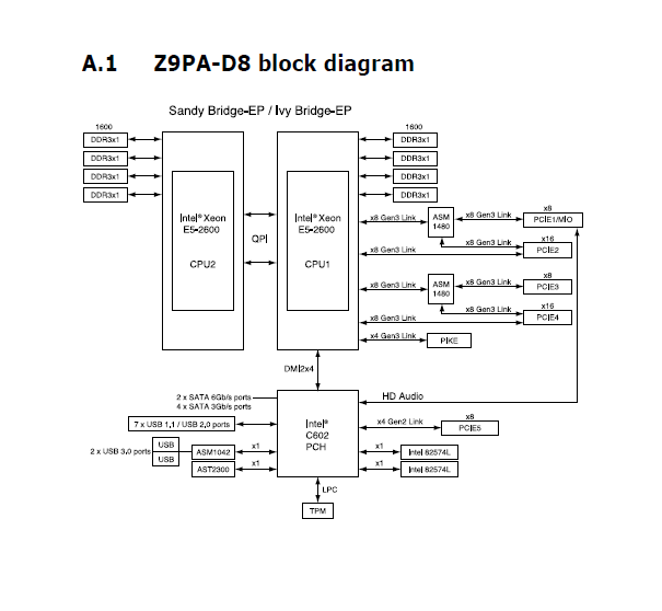
@vinclar Sadly the block diagram https://dlcdnets.asus.com/pub/ASUS/mb/So…-D8_for_web.pdf (last page) show me that dispite having 2 CPU sockets not a single x16 or x8 slot seems to get an IOU that isn’t configured by an ASM1408 or PCH chip. Your best bet would be to use a single NVME adapter.
Thanks @Jacksted for the point.
I’m not giving up yet, I will check if its posible to disable this on the bios. As I understand the ASM1480 only acts when the PCIE3 slot is used or am I wrong?
PCI Slots:
S2(PCIE1 x8 2.0): Empty
S3(PCIE2 x16 3.0): Asus Hyper M.2 x16 V2 with 4 Nvme [x8 when S4 populated]
S4(PCIE3 x8 3.0): Empty
S5(PCIE4 x16 3.0): Intel Eth 4x1Gbit [x8 when S6 populated]
S6(PCIE5 x8 3.0): LSI Raid card
SA(PIKE): Empty
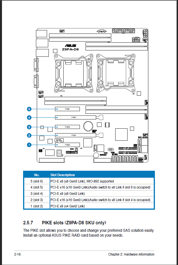
On the diagram PCIE names are mixed up with the ones on the specs and printed on the board.
Slot 2 -> PCIE1 x8 2.0 on the specs and in diagram this is -> PCIE5 x8 on Intel C602 PCH
Slot 3 ->(PCIE2 x16 3.0) in the diagram is -> PCIE4
Slot 4 ->(PCIE3 x8 3.0) in the diagram is -> PCIE3
Slot 5 ->(PCIE4 x16 3.0) in the diagram is -> PCIE2
Slot 6 ->(PCIE5 x8 3.0 MIO) in the diagram is -> PCIE1/MIO
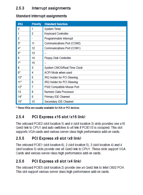
It’s hard for me to understand such design decisions: Each Ivy Bridge-EP CPU provides three PCIe Root Ports: Two with 16 lanes each and one with 8 lanes.
In the Z9PA-D8’s design it appears 4 lanes to be split off of an ×8 root port and the remaining two ×16 ports were split in four ×8’s, while leaving second CPU’s Root Ports completely unused.
The result is that none of the expansion slots is directly wired to a CPU, except for the ×4 pike slot.
On the diagram(which is misleading) on the PCIE4(x16) seems to have a direct x8 to CPU1 and a (x8) to the ASM1480 which is switched when the PCIE3 is in use.
What I don’t understand with that diagram it’s how a x16 is ever working.
The only way I think it will work it’s like the diagram only represents the switch case or I don’t know how to interprete it.
In the manual talks about shared slots:
@paranoid_android Documentation claims this:
I think the main problem with the Z9PA-D8 is that while an IOH contains 16 or 8 lanes the legacy bifurcation settings that are not exposed as in most x79 and c600(2) consumer boards assume an IOU = a PCIe slot. This in no way prohibited motherboard designers to mix and match PCIe lanes in any configuration.
In this case I believe the ASM1480’s is not a true multiplexers but a switch to reallocate PCIe lanes according to slot occupation with the limitation of one of the 2 slots being max x8. A true multiplexing PCIe chip would create extra PCIe lanes per chip and reordering PCIe packets with as an added benefit more efficiency/speed (it can make one x16 set of lanes 2 sets of x16).
For the ASM1480 this means for two PCIe slots managed by an ASM1480 you can run one card with 16 lanes or two cards with 8 lanes available. By my logic this means that for this to work the BIOS has a mechanism where the ASM1480 has a low level bios driver that tells the BIOS when to bifurcate to x8 x8 and switches 8 lanes to both PCIe slots or 16 all the to lanes to the x16 slot.
I believe it’s probable that the ASM1480 driver or the governing BIOS variable is not compatible with further bifurcation to further sets of X4 PCIe lanes.
Even though the diagram shows 8 lanes going directly to the lower x16 slot these are to enable switching very probable the last 8 lanes of the set of 16 that just stay there.
Taking all this into consideration if you were able to tell the bios to go x8x4x4 and make it stick in some way you could in theory bifurcate the last 8 lanes of the x16 slot, you just have to somehow break the mechanism of the ASM1480 setting the bifurcation of the IOU to x16 when you plop an X16 card in there (when the x8 slot isn’t occupied) and pray the ASM1480 is dumb enough to still provide a clock signal to the X16 slot.
Best case scenario here would be to able to use 2 NVME on the last 2 NVME sockets of your Asus x16 Hyper M.2 card.
I hope the amount of probables in this post convey my complete lack of complete understanding here. Nevertheless I wholeheartedly invite anyone with more knowledge, interest or patience to dive into the world of assembly, low level UEFI/BIOS driver de/recompiling and the endless joy of trial and error, to hack the marriage of a Z9PA-D8 and a Hyper M.2 x16 Card into working in some way better then just one NVME.
Well I will try the other configs x8x4x4x and x4x4x8 and let you know what happens.
I have two Hyper M.2 cards, so I could use them as a fallback config two nvme per pcie slot if this work.
Checking the extraction of the IOH using Uefitool.exe on the UEFI I found this even I set Failsafe x4x4x4x4 and optimal also x4x4x4x4 using AMIBCP v4.53 tool on the bios file.
Line 41 x16 still being the default value there.
1
2
3
4
5
6
7
8
9
10
11
12
13
14
15
16
17
18
19
20
21
22
23
24
25
26
27
28
29
30
31
32
33
34
35
36
37
38
39
40
41
42
43
44
45
46
47
48
49
50
51
52
53
54
55
56
57
58
59
60
61
62
63
64
65
66
67
68
69
70
71
72
73
74
75
76
77
78
79
80
81
82
83
84
85
86
87
88
89
90
91
92
93
94
95
96
97
98
99
100
101
102
103
104
105
106
107
108
109
110
111
112
113
114
115
116
117
118
119
120
121
122
123
124
125
126
127
128
129
130
131
132
133
134
135
136
137
138
139
140
141
142
143
144
145
146
147
148
149
150
151
152
153
154
155
156
157
158
159
160
161
162
163
164
165
166
167
168
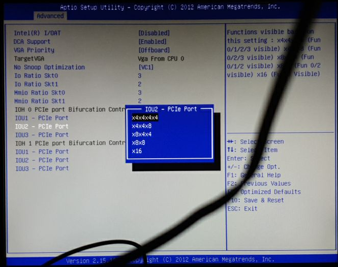
0x20C24 				Subtitle: Statement.Prompt: IOH 0 PCIe port Bifurcation Control, Flags: 0x0 {02 87 51 03 00 00 00}
0x20C2B 				End {29 02}
0x20C2D 				Subtitle: Statement.Prompt: , Flags: 0x0 {02 87 02 00 00 00 00}
0x20C34 				End {29 02}
0x20C36 			End If {29 02}
0x20C38 			Suppress If {0A 82}
0x20C3A 				True {46 02}
0x20C3C 				One Of: IOU1 - PCIe Port, VarStoreInfo (VarOffset/VarName): 0x67, VarStore: 0x1, QuestionId: 0x8A, Size: 1, Min: 0x0, Max 0x0, Step: 0x0 {05 A6 59 03 75 03 8A 00 01 00 67 00 10 10 00 00 00 00 00 00 00 00 00 00 00 00 00 00 00 00 00 00 00 00 00 00 00 00}
0x20C62 					One Of Option: x4x4, Value (8 bit): 0x0 (default) {09 0E 79 03 30 00 00 00 00 00 00 00 00 00}
0x20C70 					One Of Option: x8, Value (8 bit): 0x1 {09 0E 78 03 00 00 01 00 00 00 00 00 00 00}
0x20C7E 				End One Of {29 02}
0x20C80 			End If {29 02}
0x20C82 			Suppress If {0A 82}
0x20C84 				True {46 02}
0x20C86 				One Of: PORT 1A Link Speed, VarStoreInfo (VarOffset/VarName): 0x68, VarStore: 0x1, QuestionId: 0x8B, Size: 1, Min: 0x0, Max 0x0, Step: 0x0 {05 A6 67 03 71 03 8B 00 01 00 68 00 10 10 00 00 00 00 00 00 00 00 00 00 00 00 00 00 00 00 00 00 00 00 00 00 00 00}
0x20CAC 					One Of Option: GEN1, Value (8 bit): 0x0 {09 0E 72 03 00 00 00 00 00 00 00 00 00 00}
0x20CBA 					One Of Option: GEN2, Value (8 bit): 0x1 {09 0E 73 03 00 00 01 00 00 00 00 00 00 00}
0x20CC8 					One Of Option: GEN3, Value (8 bit): 0x2 {09 0E 74 03 00 00 02 00 00 00 00 00 00 00}
0x20CD6 					One Of Option: AUTO, Value (8 bit): 0xFF (default) {09 0E F2 05 30 00 FF 00 00 00 00 00 00 00}
0x20CE4 				End One Of {29 02}
0x20CE6 			End If {29 02}
0x20CE8 			Suppress If {0A 82}
0x20CEA 				QuestionId: 0x8A equals value 0x1 {12 86 8A 00 01 00}
0x20CF0 					True {46 02}
0x20CF2 					Or {16 02}
0x20CF4 				End {29 02}
0x20CF6 				One Of: PORT 1B Link Speed, VarStoreInfo (VarOffset/VarName): 0x6C, VarStore: 0x1, QuestionId: 0x8C, Size: 1, Min: 0x0, Max 0x0, Step: 0x0 {05 A6 68 03 71 03 8C 00 01 00 6C 00 10 10 00 00 00 00 00 00 00 00 00 00 00 00 00 00 00 00 00 00 00 00 00 00 00 00}
0x20D1C 					One Of Option: GEN1, Value (8 bit): 0x0 {09 0E 72 03 00 00 00 00 00 00 00 00 00 00}
0x20D2A 					One Of Option: GEN2, Value (8 bit): 0x1 {09 0E 73 03 00 00 01 00 00 00 00 00 00 00}
0x20D38 					One Of Option: GEN3, Value (8 bit): 0x2 {09 0E 74 03 00 00 02 00 00 00 00 00 00 00}
0x20D46 					One Of Option: AUTO, Value (8 bit): 0xFF (default) {09 0E F2 05 30 00 FF 00 00 00 00 00 00 00}
0x20D54 				End One Of {29 02}
0x20D56 			End If {29 02}
0x20D58 			Suppress If {0A 82}
0x20D5A 				True {46 02}
0x20D5C 				One Of: IOU2 - PCIe Port, VarStoreInfo (VarOffset/VarName): 0x78, VarStore: 0x1, QuestionId: 0x8D, Size: 1, Min: 0x0, Max 0x0, Step: 0x0 {05 A6 5A 03 76 03 8D 00 01 00 78 00 10 10 00 00 00 00 00 00 00 00 00 00 00 00 00 00 00 00 00 00 00 00 00 00 00 00}
0x20D82 					One Of Option: x4x4x4x4, Value (8 bit): 0x0 {09 0E 7A 03 00 00 00 00 00 00 00 00 00 00}
0x20D90 					One Of Option: x4x4x8, Value (8 bit): 0x1 {09 0E 7B 03 00 00 01 00 00 00 00 00 00 00}
0x20D9E 					One Of Option: x8x4x4, Value (8 bit): 0x2 {09 0E 7C 03 00 00 02 00 00 00 00 00 00 00}
0x20DAC 					One Of Option: x8x8, Value (8 bit): 0x3 {09 0E 7D 03 00 00 03 00 00 00 00 00 00 00}
0x20DBA 					One Of Option: x16, Value (8 bit): 0x4 (default) {09 0E 7E 03 30 00 04 00 00 00 00 00 00 00}
0x20DC8 				End One Of {29 02}
0x20DCA 			End If {29 02}
0x20DCC 			Suppress If {0A 82}
0x20DCE 				QuestionId: 0x8D equals value 0x4 {12 86 8D 00 04 00}
0x20DD4 					Not {17 02}
0x20DD6 					True {46 02}
0x20DD8 					Or {16 02}
0x20DDA 					True {46 02}
0x20DDC 					Or {16 02}
0x20DDE 				End {29 02}
0x20DE0 				One Of: PORT 2A Link Speed, VarStoreInfo (VarOffset/VarName): 0x79, VarStore: 0x1, QuestionId: 0x8E, Size: 1, Min: 0x0, Max 0x0, Step: 0x0 {05 A6 69 03 71 03 8E 00 01 00 79 00 10 10 00 00 00 00 00 00 00 00 00 00 00 00 00 00 00 00 00 00 00 00 00 00 00 00}
0x20E06 					One Of Option: GEN1, Value (8 bit): 0x0 {09 0E 72 03 00 00 00 00 00 00 00 00 00 00}
0x20E14 					One Of Option: GEN2, Value (8 bit): 0x1 {09 0E 73 03 00 00 01 00 00 00 00 00 00 00}
0x20E22 					One Of Option: GEN3, Value (8 bit): 0x2 {09 0E 74 03 00 00 02 00 00 00 00 00 00 00}
0x20E30 					One Of Option: AUTO, Value (8 bit): 0xFF (default) {09 0E F2 05 30 00 FF 00 00 00 00 00 00 00}
0x20E3E 				End One Of {29 02}
0x20E40 			End If {29 02}
0x20E42 			Suppress If {0A 82}
0x20E44 				QuestionId: 0x8D equals value 0x3 {12 86 8D 00 03 00}
0x20E4A 					Not {17 02}
0x20E4C 					True {46 02}
0x20E4E 					Or {16 02}
0x20E50 					True {46 02}
0x20E52 					Or {16 02}
0x20E54 				End {29 02}
0x20E56 				One Of: PORT 2A Link Speed, VarStoreInfo (VarOffset/VarName): 0x79, VarStore: 0x1, QuestionId: 0x8F, Size: 1, Min: 0x0, Max 0x0, Step: 0x0 {05 A6 69 03 71 03 8F 00 01 00 79 00 10 10 00 00 00 00 00 00 00 00 00 00 00 00 00 00 00 00 00 00 00 00 00 00 00 00}
0x20E7C 					One Of Option: GEN1, Value (8 bit): 0x0 {09 0E 72 03 00 00 00 00 00 00 00 00 00 00}
0x20E8A 					One Of Option: GEN2, Value (8 bit): 0x1 {09 0E 73 03 00 00 01 00 00 00 00 00 00 00}
0x20E98 					One Of Option: GEN3, Value (8 bit): 0x2 {09 0E 74 03 00 00 02 00 00 00 00 00 00 00}
0x20EA6 					One Of Option: AUTO, Value (8 bit): 0xFF (default) {09 0E F2 05 30 00 FF 00 00 00 00 00 00 00}
0x20EB4 				End One Of {29 02}
0x20EB6 				One Of: PORT 2C Link Speed, VarStoreInfo (VarOffset/VarName): 0x81, VarStore: 0x1, QuestionId: 0x90, Size: 1, Min: 0x0, Max 0x0, Step: 0x0 {05 A6 6B 03 71 03 90 00 01 00 81 00 10 10 00 00 00 00 00 00 00 00 00 00 00 00 00 00 00 00 00 00 00 00 00 00 00 00}
0x20EDC 					One Of Option: GEN1, Value (8 bit): 0x0 {09 0E 72 03 00 00 00 00 00 00 00 00 00 00}
0x20EEA 					One Of Option: GEN2, Value (8 bit): 0x1 {09 0E 73 03 00 00 01 00 00 00 00 00 00 00}
0x20EF8 					One Of Option: GEN3, Value (8 bit): 0x2 {09 0E 74 03 00 00 02 00 00 00 00 00 00 00}
0x20F06 					One Of Option: AUTO, Value (8 bit): 0xFF (default) {09 0E F2 05 30 00 FF 00 00 00 00 00 00 00}
0x20F14 				End One Of {29 02}
0x20F16 			End If {29 02}
0x20F18 			Suppress If {0A 82}
0x20F1A 				QuestionId: 0x8D equals value 0x2 {12 86 8D 00 02 00}
0x20F20 					Not {17 02}
0x20F22 					True {46 02}
0x20F24 					Or {16 02}
0x20F26 					True {46 02}
0x20F28 					Or {16 02}
0x20F2A 				End {29 02}
0x20F2C 				One Of: PORT 2A Link Speed, VarStoreInfo (VarOffset/VarName): 0x79, VarStore: 0x1, QuestionId: 0x91, Size: 1, Min: 0x0, Max 0x0, Step: 0x0 {05 A6 69 03 71 03 91 00 01 00 79 00 10 10 00 00 00 00 00 00 00 00 00 00 00 00 00 00 00 00 00 00 00 00 00 00 00 00}
0x20F52 					One Of Option: GEN1, Value (8 bit): 0x0 {09 0E 72 03 00 00 00 00 00 00 00 00 00 00}
0x20F60 					One Of Option: GEN2, Value (8 bit): 0x1 {09 0E 73 03 00 00 01 00 00 00 00 00 00 00}
0x20F6E 					One Of Option: GEN3, Value (8 bit): 0x2 {09 0E 74 03 00 00 02 00 00 00 00 00 00 00}
0x20F7C 					One Of Option: AUTO, Value (8 bit): 0xFF (default) {09 0E F2 05 30 00 FF 00 00 00 00 00 00 00}
0x20F8A 				End One Of {29 02}
0x20F8C 				One Of: PORT 2B Link Speed, VarStoreInfo (VarOffset/VarName): 0x7D, VarStore: 0x1, QuestionId: 0x92, Size: 1, Min: 0x0, Max 0x0, Step: 0x0 {05 A6 6A 03 71 03 92 00 01 00 7D 00 10 10 00 00 00 00 00 00 00 00 00 00 00 00 00 00 00 00 00 00 00 00 00 00 00 00}
0x20FB2 					One Of Option: GEN1, Value (8 bit): 0x0 {09 0E 72 03 00 00 00 00 00 00 00 00 00 00}
0x20FC0 					One Of Option: GEN2, Value (8 bit): 0x1 {09 0E 73 03 00 00 01 00 00 00 00 00 00 00}
0x20FCE 					One Of Option: GEN3, Value (8 bit): 0x2 {09 0E 74 03 00 00 02 00 00 00 00 00 00 00}
0x20FDC 					One Of Option: AUTO, Value (8 bit): 0xFF (default) {09 0E F2 05 30 00 FF 00 00 00 00 00 00 00}
0x20FEA 				End One Of {29 02}
0x20FEC 				One Of: PORT 2C Link Speed, VarStoreInfo (VarOffset/VarName): 0x81, VarStore: 0x1, QuestionId: 0x93, Size: 1, Min: 0x0, Max 0x0, Step: 0x0 {05 A6 6B 03 71 03 93 00 01 00 81 00 10 10 00 00 00 00 00 00 00 00 00 00 00 00 00 00 00 00 00 00 00 00 00 00 00 00}
0x21012 					One Of Option: GEN1, Value (8 bit): 0x0 {09 0E 72 03 00 00 00 00 00 00 00 00 00 00}
0x21020 					One Of Option: GEN2, Value (8 bit): 0x1 {09 0E 73 03 00 00 01 00 00 00 00 00 00 00}
0x2102E 					One Of Option: GEN3, Value (8 bit): 0x2 {09 0E 74 03 00 00 02 00 00 00 00 00 00 00}
0x2103C 					One Of Option: AUTO, Value (8 bit): 0xFF (default) {09 0E F2 05 30 00 FF 00 00 00 00 00 00 00}
0x2104A 				End One Of {29 02}
0x2104C 			End If {29 02}
0x2104E 			Suppress If {0A 82}
0x21050 				QuestionId: 0x8D equals value 0x1 {12 86 8D 00 01 00}
0x21056 					Not {17 02}
0x21058 					True {46 02}
0x2105A 					Or {16 02}
0x2105C 					True {46 02}
0x2105E 					Or {16 02}
0x21060 				End {29 02}
0x21062 				One Of: PORT 2A Link Speed, VarStoreInfo (VarOffset/VarName): 0x79, VarStore: 0x1, QuestionId: 0x94, Size: 1, Min: 0x0, Max 0x0, Step: 0x0 {05 A6 69 03 71 03 94 00 01 00 79 00 10 10 00 00 00 00 00 00 00 00 00 00 00 00 00 00 00 00 00 00 00 00 00 00 00 00}
0x21088 					One Of Option: GEN1, Value (8 bit): 0x0 {09 0E 72 03 00 00 00 00 00 00 00 00 00 00}
0x21096 					One Of Option: GEN2, Value (8 bit): 0x1 {09 0E 73 03 00 00 01 00 00 00 00 00 00 00}
0x210A4 					One Of Option: GEN3, Value (8 bit): 0x2 {09 0E 74 03 00 00 02 00 00 00 00 00 00 00}
0x210B2 					One Of Option: AUTO, Value (8 bit): 0xFF (default) {09 0E F2 05 30 00 FF 00 00 00 00 00 00 00}
0x210C0 				End One Of {29 02}
0x210C2 				One Of: PORT 2C Link Speed, VarStoreInfo (VarOffset/VarName): 0x81, VarStore: 0x1, QuestionId: 0x95, Size: 1, Min: 0x0, Max 0x0, Step: 0x0 {05 A6 6B 03 71 03 95 00 01 00 81 00 10 10 00 00 00 00 00 00 00 00 00 00 00 00 00 00 00 00 00 00 00 00 00 00 00 00}
0x210E8 					One Of Option: GEN1, Value (8 bit): 0x0 {09 0E 72 03 00 00 00 00 00 00 00 00 00 00}
0x210F6 					One Of Option: GEN2, Value (8 bit): 0x1 {09 0E 73 03 00 00 01 00 00 00 00 00 00 00}
0x21104 					One Of Option: GEN3, Value (8 bit): 0x2 {09 0E 74 03 00 00 02 00 00 00 00 00 00 00}
0x21112 					One Of Option: AUTO, Value (8 bit): 0xFF (default) {09 0E F2 05 30 00 FF 00 00 00 00 00 00 00}
0x21120 				End One Of {29 02}
0x21122 				One Of: PORT 2D Link Speed, VarStoreInfo (VarOffset/VarName): 0x85, VarStore: 0x1, QuestionId: 0x96, Size: 1, Min: 0x0, Max 0x0, Step: 0x0 {05 A6 6C 03 71 03 96 00 01 00 85 00 10 10 00 00 00 00 00 00 00 00 00 00 00 00 00 00 00 00 00 00 00 00 00 00 00 00}
0x21148 					One Of Option: GEN1, Value (8 bit): 0x0 {09 0E 72 03 00 00 00 00 00 00 00 00 00 00}
0x21156 					One Of Option: GEN2, Value (8 bit): 0x1 {09 0E 73 03 00 00 01 00 00 00 00 00 00 00}
0x21164 					One Of Option: GEN3, Value (8 bit): 0x2 {09 0E 74 03 00 00 02 00 00 00 00 00 00 00}
0x21172 					One Of Option: AUTO, Value (8 bit): 0xFF (default) {09 0E F2 05 30 00 FF 00 00 00 00 00 00 00}
0x21180 				End One Of {29 02}
0x21182 			End If {29 02}
0x21184 			Suppress If {0A 82}
0x21186 				QuestionId: 0x8D equals value 0x0 {12 86 8D 00 00 00}
0x2118C 					Not {17 02}
0x2118E 					True {46 02}
0x21190 					Or {16 02}
0x21192 					True {46 02}
0x21194 					Or {16 02}
0x21196 				End {29 02}
0x21198 				One Of: PORT 2A Link Speed, VarStoreInfo (VarOffset/VarName): 0x79, VarStore: 0x1, QuestionId: 0x97, Size: 1, Min: 0x0, Max 0x0, Step: 0x0 {05 A6 69 03 71 03 97 00 01 00 79 00 10 10 00 00 00 00 00 00 00 00 00 00 00 00 00 00 00 00 00 00 00 00 00 00 00 00}
0x211BE 					One Of Option: GEN1, Value (8 bit): 0x0 {09 0E 72 03 00 00 00 00 00 00 00 00 00 00}
0x211CC 					One Of Option: GEN2, Value (8 bit): 0x1 {09 0E 73 03 00 00 01 00 00 00 00 00 00 00}
0x211DA 					One Of Option: GEN3, Value (8 bit): 0x2 {09 0E 74 03 00 00 02 00 00 00 00 00 00 00}
0x211E8 					One Of Option: AUTO, Value (8 bit): 0xFF (default) {09 0E F2 05 30 00 FF 00 00 00 00 00 00 00}
0x211F6 				End One Of {29 02}
0x211F8 				One Of: PORT 2B Link Speed, VarStoreInfo (VarOffset/VarName): 0x7D, VarStore: 0x1, QuestionId: 0x98, Size: 1, Min: 0x0, Max 0x0, Step: 0x0 {05 A6 6A 03 71 03 98 00 01 00 7D 00 10 10 00 00 00 00 00 00 00 00 00 00 00 00 00 00 00 00 00 00 00 00 00 00 00 00}
0x2121E 					One Of Option: GEN1, Value (8 bit): 0x0 {09 0E 72 03 00 00 00 00 00 00 00 00 00 00}
0x2122C 					One Of Option: GEN2, Value (8 bit): 0x1 {09 0E 73 03 00 00 01 00 00 00 00 00 00 00}
0x2123A 					One Of Option: GEN3, Value (8 bit): 0x2 {09 0E 74 03 00 00 02 00 00 00 00 00 00 00}
0x21248 					One Of Option: AUTO, Value (8 bit): 0xFF (default) {09 0E F2 05 30 00 FF 00 00 00 00 00 00 00}
0x21256 				End One Of {29 02}
0x21258 				One Of: PORT 2C Link Speed, VarStoreInfo (VarOffset/VarName): 0x81, VarStore: 0x1, QuestionId: 0x99, Size: 1, Min: 0x0, Max 0x0, Step: 0x0 {05 A6 6B 03 71 03 99 00 01 00 81 00 10 10 00 00 00 00 00 00 00 00 00 00 00 00 00 00 00 00 00 00 00 00 00 00 00 00}
0x2127E 					One Of Option: GEN1, Value (8 bit): 0x0 {09 0E 72 03 00 00 00 00 00 00 00 00 00 00}
0x2128C 					One Of Option: GEN2, Value (8 bit): 0x1 {09 0E 73 03 00 00 01 00 00 00 00 00 00 00}
0x2129A 					One Of Option: GEN3, Value (8 bit): 0x2 {09 0E 74 03 00 00 02 00 00 00 00 00 00 00}
0x212A8 					One Of Option: AUTO, Value (8 bit): 0xFF (default) {09 0E F2 05 30 00 FF 00 00 00 00 00 00 00}
0x212B6 				End One Of {29 02}
0x212B8 				One Of: PORT 2D Link Speed, VarStoreInfo (VarOffset/VarName): 0x85, VarStore: 0x1, QuestionId: 0x9A, Size: 1, Min: 0x0, Max 0x0, Step: 0x0 {05 A6 6C 03 71 03 9A 00 01 00 85 00 10 10 00 00 00 00 00 00 00 00 00 00 00 00 00 00 00 00 00 00 00 00 00 00 00 00}
0x212DE 					One Of Option: GEN1, Value (8 bit): 0x0 {09 0E 72 03 00 00 00 00 00 00 00 00 00 00}
0x212EC 					One Of Option: GEN2, Value (8 bit): 0x1 {09 0E 73 03 00 00 01 00 00 00 00 00 00 00}
0x212FA 					One Of Option: GEN3, Value (8 bit): 0x2 {09 0E 74 03 00 00 02 00 00 00 00 00 00 00}
0x21308 					One Of Option: AUTO, Value (8 bit): 0xFF (default) {09 0E F2 05 30 00 FF 00 00 00 00 00 00 00}
0x21316 				End One Of {29 02}
0x21318 			End If {29 02}
0x2131A 			Suppress If {0A 82}
0x2131C 				True {46 02}
Hi guys,
I tried every single configuration config with 4, 3, 2, 1 and 0 expansion cards.
And predicted by your knowledge was an IM.
Found an incompatibilty mixing the LSI card and Intel on same IOU and the Intel wasn’t detected by the board.
I found that the order of the names are mixed everywhere:
IOU1 -> x8(x4/x4) PCIE5 2.0 and PIKE 3.0
IOU2 -> x16(x8/x8) PCIE3 x8 3.0 and PCIE4 x16 3.0
IOU3 -> x16(x8/x8) PCIE1/MIO x8 3.0 and PCIE2 x16 3.0
I’m considering a PLX card like HighPoint SSD7101A-1 $$$$, no limit on x16 link to cpu or an Asmedia 2824 x8 link to cpu $$.
Any recomendation? Thanks.
Changing the board is even more expensive.
1
2
3
4
5
6
7
8
9
10
11
12
13
14
15
16
17
2
3
4
5
6
7
8
9
10
11
12
13
14
15
16
17
 \-[0000:00]-+-00.0  Intel Corporation Xeon E7 v2/Xeon E5 v2/Core i7 DMI2
             +-01.0-[01]--
             +-02.0-[02]----00.0  Sandisk Corp Device 5002
             +-03.0-[03]--+-00.0  Intel Corporation 82580 Gigabit Network Connection
             |            +-00.1  Intel Corporation 82580 Gigabit Network Connection
             |            +-00.2  Intel Corporation 82580 Gigabit Network Connection
             |            \-00.3  Intel Corporation 82580 Gigabit Network Connection

             +-11.0-[04]--

             +-1c.0-[05]----00.0  LSI Logic / Symbios Logic MegaRAID SAS 2208 [Thunderbolt]
             +-1c.4-[06]----00.0  Intel Corporation 82574L Gigabit Network Connection
             +-1c.5-[07]----00.0  Intel Corporation 82574L Gigabit Network Connection
             +-1c.6-[08]----00.0  ASMedia Technology Inc. ASM1042 SuperSpeed USB Host Controller
             +-1c.7-[09-0a]----00.0-[0a]----00.0  ASPEED Technology, Inc. ASPEED Graphics Family
Full lspci tree
1
2
3
4
5
6
7
8
9
10
11
12
13
14
15
16
17
18
19
20
21
22
23
24
25
26
27
28
29
30
31
32
33
34
35
36
37
38
39
40
41
42
43
44
45
46
47
48
49
50
51
52
53
54
55
56
57
58
59
60
61
62
63
64
65
66
67
68
69
70
71
72
73
74
75
76
77
78
79
80
81
82
83
84
85
86
87
88
89
90
91
92
93
94
95
96
97
98
99
100
101
102
103
104
105
106
107
108
109
110
111
112
113
114
115
116
117
118
119
120
121
122
123
124
125
126
127
128
129
130
131
132
133
134
135
136
137
138
root:~# lspci -tvv
-+-[0000:ff]-+-08.0  Intel Corporation Xeon E7 v2/Xeon E5 v2/Core i7 QPI Link 0
 |           +-09.0  Intel Corporation Xeon E7 v2/Xeon E5 v2/Core i7 QPI Link 1
 |           +-0a.0  Intel Corporation Xeon E7 v2/Xeon E5 v2/Core i7 Power Control Unit 0
 |           +-0a.1  Intel Corporation Xeon E7 v2/Xeon E5 v2/Core i7 Power Control Unit 1
 |           +-0a.2  Intel Corporation Xeon E7 v2/Xeon E5 v2/Core i7 Power Control Unit 2
 |           +-0a.3  Intel Corporation Xeon E7 v2/Xeon E5 v2/Core i7 Power Control Unit 3
 |           +-0b.0  Intel Corporation Xeon E7 v2/Xeon E5 v2/Core i7 UBOX Registers
 |           +-0b.3  Intel Corporation Xeon E7 v2/Xeon E5 v2/Core i7 UBOX Registers
 |           +-0c.0  Intel Corporation Xeon E7 v2/Xeon E5 v2/Core i7 Unicast Registers
 |           +-0c.1  Intel Corporation Xeon E7 v2/Xeon E5 v2/Core i7 Unicast Registers
 |           +-0c.2  Intel Corporation Xeon E7 v2/Xeon E5 v2/Core i7 Unicast Registers
 |           +-0c.3  Intel Corporation Xeon E7 v2/Xeon E5 v2/Core i7 Unicast Registers
 |           +-0c.4  Intel Corporation Xeon E7 v2/Xeon E5 v2/Core i7 Unicast Registers
 |           +-0d.0  Intel Corporation Xeon E7 v2/Xeon E5 v2/Core i7 Unicast Registers
 |           +-0d.1  Intel Corporation Xeon E7 v2/Xeon E5 v2/Core i7 Unicast Registers
 |           +-0d.2  Intel Corporation Xeon E7 v2/Xeon E5 v2/Core i7 Unicast Registers
 |           +-0d.3  Intel Corporation Xeon E7 v2/Xeon E5 v2/Core i7 Unicast Registers
 |           +-0d.4  Intel Corporation Xeon E7 v2/Xeon E5 v2/Core i7 Unicast Registers
 |           +-0e.0  Intel Corporation Xeon E7 v2/Xeon E5 v2/Core i7 Home Agent 0
 |           +-0e.1  Intel Corporation Xeon E7 v2/Xeon E5 v2/Core i7 Home Agent 0
 |           +-0f.0  Intel Corporation Xeon E7 v2/Xeon E5 v2/Core i7 Integrated Memory Controller 0 Target Address/Thermal Registers
 |           +-0f.1  Intel Corporation Xeon E7 v2/Xeon E5 v2/Core i7 Integrated Memory Controller 0 RAS Registers
 |           +-0f.2  Intel Corporation Xeon E7 v2/Xeon E5 v2/Core i7 Integrated Memory Controller 0 Channel Target Address Decoder Registers
 |           +-0f.3  Intel Corporation Xeon E7 v2/Xeon E5 v2/Core i7 Integrated Memory Controller 0 Channel Target Address Decoder Registers
 |           +-0f.4  Intel Corporation Xeon E7 v2/Xeon E5 v2/Core i7 Integrated Memory Controller 0 Channel Target Address Decoder Registers
 |           +-0f.5  Intel Corporation Xeon E7 v2/Xeon E5 v2/Core i7 Integrated Memory Controller 0 Channel Target Address Decoder Registers
 |           +-10.0  Intel Corporation Xeon E7 v2/Xeon E5 v2/Core i7 Integrated Memory Controller 1 Channel 0-3 Thermal Control 0
 |           +-10.1  Intel Corporation Xeon E7 v2/Xeon E5 v2/Core i7 Integrated Memory Controller 1 Channel 0-3 Thermal Control 1
 |           +-10.2  Intel Corporation Xeon E7 v2/Xeon E5 v2/Core i7 Integrated Memory Controller 1 Channel 0-3 ERROR Registers 0
 |           +-10.3  Intel Corporation Xeon E7 v2/Xeon E5 v2/Core i7 Integrated Memory Controller 1 Channel 0-3 ERROR Registers 1
 |           +-10.4  Intel Corporation Xeon E7 v2/Xeon E5 v2/Core i7 Integrated Memory Controller 1 Channel 0-3 Thermal Control 2
 |           +-10.5  Intel Corporation Xeon E7 v2/Xeon E5 v2/Core i7 Integrated Memory Controller 1 Channel 0-3 Thermal Control 3
 |           +-10.6  Intel Corporation Xeon E7 v2/Xeon E5 v2/Core i7 Integrated Memory Controller 1 Channel 0-3 ERROR Registers 2
 |           +-10.7  Intel Corporation Xeon E7 v2/Xeon E5 v2/Core i7 Integrated Memory Controller 1 Channel 0-3 ERROR Registers 3
 |           +-13.0  Intel Corporation Xeon E7 v2/Xeon E5 v2/Core i7 R2PCIe
 |           +-13.1  Intel Corporation Xeon E7 v2/Xeon E5 v2/Core i7 R2PCIe
 |           +-13.4  Intel Corporation Xeon E7 v2/Xeon E5 v2/Core i7 QPI Ring Registers
 |           +-13.5  Intel Corporation Xeon E7 v2/Xeon E5 v2/Core i7 QPI Ring Performance Ring Monitoring
 |           +-16.0  Intel Corporation Xeon E7 v2/Xeon E5 v2/Core i7 System Address Decoder
 |           +-16.1  Intel Corporation Xeon E7 v2/Xeon E5 v2/Core i7 Broadcast Registers
 |           \-16.2  Intel Corporation Xeon E7 v2/Xeon E5 v2/Core i7 Broadcast Registers
 +-[0000:80]-+-00.0-[81]--
 |           +-01.0-[82]--
 |           +-02.0-[83]--
 |           +-02.1-[84]--
 |           +-02.2-[85]--
 |           +-02.3-[86]--
 |           +-03.0-[87]--
 |           +-03.1-[88]--
 |           +-03.2-[89]--
 |           +-03.3-[8a]--
 |           +-04.0  Intel Corporation Xeon E7 v2/Xeon E5 v2/Core i7 Crystal Beach DMA Channel 0
 |           +-04.1  Intel Corporation Xeon E7 v2/Xeon E5 v2/Core i7 Crystal Beach DMA Channel 1
 |           +-04.2  Intel Corporation Xeon E7 v2/Xeon E5 v2/Core i7 Crystal Beach DMA Channel 2
 |           +-04.3  Intel Corporation Xeon E7 v2/Xeon E5 v2/Core i7 Crystal Beach DMA Channel 3
 |           +-04.4  Intel Corporation Xeon E7 v2/Xeon E5 v2/Core i7 Crystal Beach DMA Channel 4
 |           +-04.5  Intel Corporation Xeon E7 v2/Xeon E5 v2/Core i7 Crystal Beach DMA Channel 5
 |           +-04.6  Intel Corporation Xeon E7 v2/Xeon E5 v2/Core i7 Crystal Beach DMA Channel 6
 |           +-04.7  Intel Corporation Xeon E7 v2/Xeon E5 v2/Core i7 Crystal Beach DMA Channel 7
 |           +-05.0  Intel Corporation Xeon E7 v2/Xeon E5 v2/Core i7 VTd/Memory Map/Misc
 |           +-05.2  Intel Corporation Xeon E7 v2/Xeon E5 v2/Core i7 IIO RAS
 |           \-05.4  Intel Corporation Xeon E7 v2/Xeon E5 v2/Core i7 IOAPIC
 +-[0000:7f]-+-08.0  Intel Corporation Xeon E7 v2/Xeon E5 v2/Core i7 QPI Link 0
 |           +-09.0  Intel Corporation Xeon E7 v2/Xeon E5 v2/Core i7 QPI Link 1
 |           +-0a.0  Intel Corporation Xeon E7 v2/Xeon E5 v2/Core i7 Power Control Unit 0
 |           +-0a.1  Intel Corporation Xeon E7 v2/Xeon E5 v2/Core i7 Power Control Unit 1
 |           +-0a.2  Intel Corporation Xeon E7 v2/Xeon E5 v2/Core i7 Power Control Unit 2
 |           +-0a.3  Intel Corporation Xeon E7 v2/Xeon E5 v2/Core i7 Power Control Unit 3
 |           +-0b.0  Intel Corporation Xeon E7 v2/Xeon E5 v2/Core i7 UBOX Registers
 |           +-0b.3  Intel Corporation Xeon E7 v2/Xeon E5 v2/Core i7 UBOX Registers
 |           +-0c.0  Intel Corporation Xeon E7 v2/Xeon E5 v2/Core i7 Unicast Registers
 |           +-0c.1  Intel Corporation Xeon E7 v2/Xeon E5 v2/Core i7 Unicast Registers
 |           +-0c.2  Intel Corporation Xeon E7 v2/Xeon E5 v2/Core i7 Unicast Registers
 |           +-0c.3  Intel Corporation Xeon E7 v2/Xeon E5 v2/Core i7 Unicast Registers
 |           +-0c.4  Intel Corporation Xeon E7 v2/Xeon E5 v2/Core i7 Unicast Registers
 |           +-0d.0  Intel Corporation Xeon E7 v2/Xeon E5 v2/Core i7 Unicast Registers
 |           +-0d.1  Intel Corporation Xeon E7 v2/Xeon E5 v2/Core i7 Unicast Registers
 |           +-0d.2  Intel Corporation Xeon E7 v2/Xeon E5 v2/Core i7 Unicast Registers
 |           +-0d.3  Intel Corporation Xeon E7 v2/Xeon E5 v2/Core i7 Unicast Registers
 |           +-0d.4  Intel Corporation Xeon E7 v2/Xeon E5 v2/Core i7 Unicast Registers
 |           +-0e.0  Intel Corporation Xeon E7 v2/Xeon E5 v2/Core i7 Home Agent 0
 |           +-0e.1  Intel Corporation Xeon E7 v2/Xeon E5 v2/Core i7 Home Agent 0
 |           +-0f.0  Intel Corporation Xeon E7 v2/Xeon E5 v2/Core i7 Integrated Memory Controller 0 Target Address/Thermal Registers
 |           +-0f.1  Intel Corporation Xeon E7 v2/Xeon E5 v2/Core i7 Integrated Memory Controller 0 RAS Registers
 |           +-0f.2  Intel Corporation Xeon E7 v2/Xeon E5 v2/Core i7 Integrated Memory Controller 0 Channel Target Address Decoder Registers
 |           +-0f.3  Intel Corporation Xeon E7 v2/Xeon E5 v2/Core i7 Integrated Memory Controller 0 Channel Target Address Decoder Registers
 |           +-0f.4  Intel Corporation Xeon E7 v2/Xeon E5 v2/Core i7 Integrated Memory Controller 0 Channel Target Address Decoder Registers
 |           +-0f.5  Intel Corporation Xeon E7 v2/Xeon E5 v2/Core i7 Integrated Memory Controller 0 Channel Target Address Decoder Registers
 |           +-10.0  Intel Corporation Xeon E7 v2/Xeon E5 v2/Core i7 Integrated Memory Controller 1 Channel 0-3 Thermal Control 0
 |           +-10.1  Intel Corporation Xeon E7 v2/Xeon E5 v2/Core i7 Integrated Memory Controller 1 Channel 0-3 Thermal Control 1
 |           +-10.2  Intel Corporation Xeon E7 v2/Xeon E5 v2/Core i7 Integrated Memory Controller 1 Channel 0-3 ERROR Registers 0
 |           +-10.3  Intel Corporation Xeon E7 v2/Xeon E5 v2/Core i7 Integrated Memory Controller 1 Channel 0-3 ERROR Registers 1
 |           +-10.4  Intel Corporation Xeon E7 v2/Xeon E5 v2/Core i7 Integrated Memory Controller 1 Channel 0-3 Thermal Control 2
 |           +-10.5  Intel Corporation Xeon E7 v2/Xeon E5 v2/Core i7 Integrated Memory Controller 1 Channel 0-3 Thermal Control 3
 |           +-10.6  Intel Corporation Xeon E7 v2/Xeon E5 v2/Core i7 Integrated Memory Controller 1 Channel 0-3 ERROR Registers 2
 |           +-10.7  Intel Corporation Xeon E7 v2/Xeon E5 v2/Core i7 Integrated Memory Controller 1 Channel 0-3 ERROR Registers 3
 |           +-13.0  Intel Corporation Xeon E7 v2/Xeon E5 v2/Core i7 R2PCIe
 |           +-13.1  Intel Corporation Xeon E7 v2/Xeon E5 v2/Core i7 R2PCIe
 |           +-13.4  Intel Corporation Xeon E7 v2/Xeon E5 v2/Core i7 QPI Ring Registers
 |           +-13.5  Intel Corporation Xeon E7 v2/Xeon E5 v2/Core i7 QPI Ring Performance Ring Monitoring
 |           +-16.0  Intel Corporation Xeon E7 v2/Xeon E5 v2/Core i7 System Address Decoder
 |           +-16.1  Intel Corporation Xeon E7 v2/Xeon E5 v2/Core i7 Broadcast Registers
 |           \-16.2  Intel Corporation Xeon E7 v2/Xeon E5 v2/Core i7 Broadcast Registers
 \-[0000:00]-+-00.0  Intel Corporation Xeon E7 v2/Xeon E5 v2/Core i7 DMI2
             +-01.0-[01]--
             +-02.0-[02]----00.0  Sandisk Corp Device 5002
             +-03.0-[03]--+-00.0  Intel Corporation 82580 Gigabit Network Connection
             |            +-00.1  Intel Corporation 82580 Gigabit Network Connection
             |            +-00.2  Intel Corporation 82580 Gigabit Network Connection
             |            \-00.3  Intel Corporation 82580 Gigabit Network Connection
             +-04.0  Intel Corporation Xeon E7 v2/Xeon E5 v2/Core i7 Crystal Beach DMA Channel 0
             +-04.1  Intel Corporation Xeon E7 v2/Xeon E5 v2/Core i7 Crystal Beach DMA Channel 1
             +-04.2  Intel Corporation Xeon E7 v2/Xeon E5 v2/Core i7 Crystal Beach DMA Channel 2
             +-04.3  Intel Corporation Xeon E7 v2/Xeon E5 v2/Core i7 Crystal Beach DMA Channel 3
             +-04.4  Intel Corporation Xeon E7 v2/Xeon E5 v2/Core i7 Crystal Beach DMA Channel 4
             +-04.5  Intel Corporation Xeon E7 v2/Xeon E5 v2/Core i7 Crystal Beach DMA Channel 5
             +-04.6  Intel Corporation Xeon E7 v2/Xeon E5 v2/Core i7 Crystal Beach DMA Channel 6
             +-04.7  Intel Corporation Xeon E7 v2/Xeon E5 v2/Core i7 Crystal Beach DMA Channel 7
             +-05.0  Intel Corporation Xeon E7 v2/Xeon E5 v2/Core i7 VTd/Memory Map/Misc
             +-05.2  Intel Corporation Xeon E7 v2/Xeon E5 v2/Core i7 IIO RAS
             +-05.4  Intel Corporation Xeon E7 v2/Xeon E5 v2/Core i7 IOAPIC
             +-11.0-[04]--
             +-16.0  Intel Corporation C600/X79 series chipset MEI Controller #1
             +-16.1  Intel Corporation C600/X79 series chipset MEI Controller #2
             +-1a.0  Intel Corporation C600/X79 series chipset USB2 Enhanced Host Controller #2
             +-1c.0-[05]----00.0  LSI Logic / Symbios Logic MegaRAID SAS 2208 [Thunderbolt]
             +-1c.4-[06]----00.0  Intel Corporation 82574L Gigabit Network Connection
             +-1c.5-[07]----00.0  Intel Corporation 82574L Gigabit Network Connection
             +-1c.6-[08]----00.0  ASMedia Technology Inc. ASM1042 SuperSpeed USB Host Controller
             +-1c.7-[09-0a]----00.0-[0a]----00.0  ASPEED Technology, Inc. ASPEED Graphics Family
             +-1d.0  Intel Corporation C600/X79 series chipset USB2 Enhanced Host Controller #1
             +-1e.0-[0b]--
             +-1f.0  Intel Corporation C600/X79 series chipset LPC Controller
             +-1f.2  Intel Corporation C600/X79 series chipset 6-Port SATA AHCI Controller
             \-1f.3  Intel Corporation C600/X79 series chipset SMBus Host Controller
@vinclar
If you can fit the board https://www.ebay.com/itm/Supermicro-X9DR…JYAAOSwwkxdk9bc
Seems to work with updated bios. hash=item1f067f81ac:g:v6cAAOSwD0dd3cUr https://www.reddit.com/r/homelab/comment…_on_supermicro/
Thanks @JackSted for the suggestion and resource. I’m located at Spain. From US it would take some time and this one only supports V1 CPU version.
I already wrote to Asus support just to have a chance.
The case is this Chenbro RM42200 max size is Supports M/B up to 12” x 10.5”
Hi guys, I decided to try a card named, SI-PEX40152 or IO-SI-PEX40152, wich equips a PM8562 PFX-L 32XG3 chip, at a half price of a HighPoint SSD7101A-1
It’s like the ASUS but with a chip for bifuracation a x16 direct lane to cpu and does the job.
I thinks it’s the best solution due the case of the lack of support of bifurcation cause of the restrictive implementation of the the ASM1480 switch or just not being implemented.
@vinclar Glad to hear you possibly found a solution. Let us know if it all works out ![]()