I own a Lenovo Ideapad Y700 15isk. The bios is secured and, apparently, unsigned (modded) bioses cannot be flashed; only a SPI programmer is possible. I am trying to circumvent this as I have no access to this tool where I live - Ghana. I have dug around a bit and discovered certain interesting things I want to share with you so that you could offer me your opinion concerning possibilities/options.
My current ME Info Summary is as follows:
Intel ME FW Version: 11.0.0.1202 H
Intel ME Recovery Image Version: 11.0.0.1202
Intel ME FITC Version: 11.0.0.1202
My ultimate goal is to unlock the advanced menu and other hidden features in the ME and then reflash through normal method.
Lenovo has released a good number of bioses, but with an older version 3.5, which was quickly pulled, they also included an upgrade of the ME FW to 11.0.0.1202. I don’t know if it is as a result of this upgrade, but the flashing of this particular 3.5 bios was unusual. I flashed the bios in Windows 10 x64 Pro. The system rebooted 5 times as part of the bios upgrade and process. The phases are as follows:
Phase 1: UAC disabling (registry edit and reboot)
Phase 2: ME “Unlock” (reboot)
Phase 3: Bios FW loading (reboot and flashing)
Phase 4: UAC enabling (registry edit and reboot)
Phase 5: Confirmation of success
During the second cycle, I noticed an eye-popping “ME Unlock” in the sequence of lines displayed in the CMD window. So I unpacked the package and found a number of files with two batch files; “setup.bat,” and “process.bat” among them. The setup.bat initiates the process, as follows:
echo Step 1: tun off UAC
echo y | reg add “HKLM\Software\Microsoft\Windows\CurrentVersion\Policies\System” /v EnableLUA /t REG_DWORD /d 0 /f>nul
if %errorlevel%==1 set ERRORMSG=Could not disable UAC && goto ERROR
reg add “HKCU\Software\Microsoft\Windows\CurrentVersion\Explorer\Advanced” /v “EnableXamlStartMenu” /t REG_DWORD /d “0” /f
@copy /y %Temp%\ThreeFlash\Process.bat %Userprofile%\AppData\Roaming\Microsoft\Windows"Start Menu"\Programs\Startup\Process.bat > nul
Shutdown.exe -r
goto end
On the next boot, process.bat kicks into action with the following line:
echo Step 2: Unlock ME before flash BIOS and EC!
cd %Temp%\ThreeFlash
WinTest.exe C45 D80
WinTest.exe C40 D02
A little something on this;
WinTest.exe C45 D80 unlocks the ME. Even though it says unlock, it seems more like shutdown, I suppose in preparation for the upgrade because after this command is issued the ME is unresponsive to any commands. MEInfo, MEManuf, and FWUpdLcl64 all don’t work. I lose audio after the reboot.
WinTest.exe C40 D02 reboots the system.
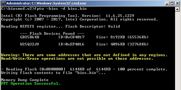
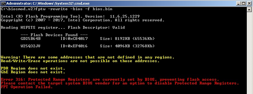
After observing this, I replicated the UAC off, reboot, ME unlock, reboot, and dumped my entire bios with the flashing app, H2OFFT-Wx64 using the ‘BackupROM’ flag. I then reversed the process, as detailed in the batch files.
Audio was restored again with a WinTest.exe C45 D81 command, and a system reboot.
My question is, with the “unlocked” ME dumped bios, is it possible that the ME could be in a vulnerable state where its settings could be changed? Since it’s totally unresponsive in a live system, could it be extracted and settings edited to unlock it permanently, injected back and possibly flashed back while the system is rendered receptive again - ie. UAC off, ME unlocked? Is this worth a shot? It appears the ME unlock procedure is only necessary for the upgrade of the ME firmware and so has nothing to do with the secure-flash protection mechanisms of the rest of bios, but I want to believe that the ME itself can offer a backdoor into the castle. 
Please advice. I have all the files and would be glad if the geniuses in the community could look into this.
PS: I did manage to upgrade my ME FW to version 11.6, but FITC version still remained 11.0. I’ve since reverted back with a fresh bios update. While on 11.6, I got some errors (yellow text) in MEManuf. Also, I couldn’t downgrade or revert to 11.0 using FWUpdLcl64. Only a bios reflash did the trick.
Thank you.
Here is a MEInfo report of my system:
Copyright(C) 2005 - 2016, Intel Corporation. All rights reserved.
FW Status Register1: 0x90000245
FW Status Register2: 0x06F60506
FW Status Register3: 0x00000200
FW Status Register4: 0x00084000
FW Status Register5: 0x00000000
FW Status Register6: 0x40000000
CurrentState: Normal
ManufacturingMode: Disabled
FlashPartition: Valid
OperationalState: CM0 with UMA
InitComplete: Complete
BUPLoadState: Success
ErrorCode: No Error
ModeOfOperation: Normal
SPI Flash Log: Not Present
Phase: ROM/Preboot
ICC: Valid OEM data, ICC programmed
ME File System Corrupted: No
PhaseStatus: AFTER_SRAM_INIT
FPF and ME Config Status: Match
FW Capabilities value is 0x31111940
Feature enablement is 0x31111940
Platform type is 0x11220321
Found an Intel vPro Wireless device
Intel(R) ME code versions:
Windows OS Version : 6.2.9200 “”
Table Type 0 ( 0x 00 ) found, size of 24 (0x 18 ) bytes
BIOS Version CDCN35WW
Windows OS Version : 6.2.9200 “”
Table Type 0 ( 0x 00 ) found, size of 24 (0x 18 ) bytes
Table Type 1 ( 0x 01 ) found, size of 27 (0x 1B ) bytes
Table Type 2 ( 0x 02 ) found, size of 15 (0x 0F ) bytes
Table Type 3 ( 0x 03 ) found, size of 22 (0x 16 ) bytes
Table Type 4 ( 0x 04 ) found, size of 42 (0x 2A ) bytes
Table Type 7 ( 0x 07 ) found, size of 19 (0x 13 ) bytes
Table Type 7 ( 0x 07 ) found, size of 19 (0x 13 ) bytes
Table Type 7 ( 0x 07 ) found, size of 19 (0x 13 ) bytes
Table Type 7 ( 0x 07 ) found, size of 19 (0x 13 ) bytes
Table Type 8 ( 0x 08 ) found, size of 9 (0x 09 ) bytes
Table Type 8 ( 0x 08 ) found, size of 9 (0x 09 ) bytes
Table Type 8 ( 0x 08 ) found, size of 9 (0x 09 ) bytes
Table Type 8 ( 0x 08 ) found, size of 9 (0x 09 ) bytes
Table Type 8 ( 0x 08 ) found, size of 9 (0x 09 ) bytes
Table Type 8 ( 0x 08 ) found, size of 9 (0x 09 ) bytes
Table Type 8 ( 0x 08 ) found, size of 9 (0x 09 ) bytes
Table Type 8 ( 0x 08 ) found, size of 9 (0x 09 ) bytes
Table Type 8 ( 0x 08 ) found, size of 9 (0x 09 ) bytes
Table Type 9 ( 0x 09 ) found, size of 17 (0x 11 ) bytes
Table Type 9 ( 0x 09 ) found, size of 17 (0x 11 ) bytes
Table Type 9 ( 0x 09 ) found, size of 17 (0x 11 ) bytes
Table Type 9 ( 0x 09 ) found, size of 17 (0x 11 ) bytes
Table Type 9 ( 0x 09 ) found, size of 17 (0x 11 ) bytes
Table Type 13 ( 0x 0D ) found, size of 22 (0x 16 ) bytes
Table Type 14 ( 0x 0E ) found, size of 17 (0x 11 ) bytes
Table Type 14 ( 0x 0E ) found, size of 8 (0x 08 ) bytes
Table Type 14 ( 0x 0E ) found, size of 8 (0x 08 ) bytes
Table Type 15 ( 0x 0F ) found, size of 29 (0x 1D ) bytes
Table Type 16 ( 0x 10 ) found, size of 23 (0x 17 ) bytes
Table Type 17 ( 0x 11 ) found, size of 40 (0x 28 ) bytes
Table Type 17 ( 0x 11 ) found, size of 40 (0x 28 ) bytes
Table Type 17 ( 0x 11 ) found, size of 40 (0x 28 ) bytes
Table Type 17 ( 0x 11 ) found, size of 40 (0x 28 ) bytes
Table Type 19 ( 0x 13 ) found, size of 31 (0x 1F ) bytes
Table Type 20 ( 0x 14 ) found, size of 35 (0x 23 ) bytes
Table Type 20 ( 0x 14 ) found, size of 35 (0x 23 ) bytes
Table Type 21 ( 0x 15 ) found, size of 7 (0x 07 ) bytes
Table Type 24 ( 0x 18 ) found, size of 5 (0x 05 ) bytes
Table Type 133 ( 0x 85 ) found, size of 5 (0x 05 ) bytes
Table Type 200 ( 0x C8 ) found, size of 16 (0x 10 ) bytes
Table Type 219 ( 0x DB ) found, size of 81 (0x 51 ) bytes
Table Type 221 ( 0x DD ) found, size of 26 (0x 1A ) bytes
Table Type 221 ( 0x DD ) found, size of 26 (0x 1A ) bytes
Table Type 221 ( 0x DD ) found, size of 68 (0x 44 ) bytes
Table Type 221 ( 0x DD ) found, size of 54 (0x 36 ) bytes
Table Type 222 ( 0x DE ) found, size of 14 (0x 0E ) bytes
Table Type 248 ( 0x F8 ) found, size of 18 (0x 12 ) bytes
Table Type 127 ( 0x 7F ) found, size of 4 (0x 04 ) bytes
SM BIOS table entry point structure not found
MEBx Version Not Available
GbE Region does not exist.
GbE Version Unknown
Vendor ID 8086
PCH Version 31
FW Version 11.0.0.1202 H
LMS Version Not Available
MEI Driver Version 11.5.0.1011
Wireless Hardware Version 2.1.77
Wireless Driver Version 19.30.0.4
FW Capabilities 0x31111940
Intel(R) Capability Licensing Service - PRESENT/ENABLED
Protect Audio Video Path - PRESENT/ENABLED
Intel(R) Dynamic Application Loader - PRESENT/ENABLED
Service Advertisement & Discovery - NOT PRESENT
Intel(R) NFC Capabilities - NOT PRESENT
Intel(R) Platform Trust Technology - PRESENT/ENABLED
TLS Disabled
Last ME reset reason Firmware reset
Local FWUpdate Enabled
BIOS Config Lock Enabled
GbE Config Lock Enabled
Get flash master region access status…done
Host Read Access to ME Disabled
Host Write Access to ME Disabled
Get EC region access status…done
Host Read Access to EC Enabled
Host Write Access to EC Enabled
Protected Range Register Base #0 0x6C0
Protected Range Register Limit #0 0x7FF
Protected Range Register Base #1 0x29A
Protected Range Register Limit #1 0x57F
Protected Range Register Base #2 0x0
Protected Range Register Limit #2 0x0
Protected Range Register Base #3 0x0
Protected Range Register Limit #3 0x0
Protected Range Register Base #4 0x0
Protected Range Register Limit #4 0x0
SPI Flash ID 1 C84017
SPI Flash ID 2 Unknown
BIOS boot State Post Boot
OEM ID 00000000-0000-0000-0000-000000000000
Capability Licensing Service Enabled
OEM Tag 0x00000000
Slot 1 Board Manufacturer 0x00000000
Slot 2 System Assembler 0x00000000
Slot 3 Reserved 0x00000000
M3 Autotest Disabled
C-link Status Disabled
Independent Firmware Recovery Disabled
EPID Group ID 0xF8D
OEM Public Key Hash FPF 0000000000000000000000000000000000000000000000000000000000000000
Retrieving Variable "OEM Public Key Hash"
OEM Public Key Hash ME 0000000000000000000000000000000000000000000000000000000000000000
ACM SVN FPF 0x0
KM SVN FPF 0x0
BSMM SVN FPF 0x0
GuC Encryption Key FPF 0000000000000000000000000000000000000000000000000000000000000000
Retrieving Variable "GuC Encryption Key"
GuC Encryption Key ME 0000000000000000000000000000000000000000000000000000000000000000
FPF ME
— –
Force Boot Guard ACM Disabled
Retrieving Variable “Force Boot Guard ACM Enabled” Disabled
Protect BIOS Environment Disabled
Retrieving Variable “Protect BIOS Environment Enabled” Disabled
CPU Debugging Enabled
Retrieving Variable “CPU Debugging” Enabled
BSP Initialization Enabled
Retrieving Variable “BSP Initialization” Enabled
Measured Boot Disabled
Retrieving Variable “Measured Boot Enabled” Disabled
Verified Boot Disabled
Retrieving Variable “Verified Boot Enabled” Disabled
Key Manifest ID 0x0
Retrieving Variable “Key Manifest ID” 0x0
Enforcement Policy 0x0
Retrieving Variable “Error Enforcement Policy” 0x0
PTT Enabled
Retrieving Variable “Intel(R) PTT Supported” Enabled
PTT Lockout Override Counter 0x0
EK Revoke State Not Revoked
PTT RTC Clear Detection FPF 0x0
I used another tool to dump my current default settings. Here’s a snippet:
********** OverClocking Performance Menu
(0x2E4, 1, 0x61D25395F30E92B3) OverClocking Feature
Callback ID = 0x3f
(0)[] Disabled (Default)
(1)[ ] Enabled
(0x2E5, 1, 0x61D25395F30E92B3) IMON Scaling Support
Callback ID = 0x40
(0)[] Disabled (Default)
(1)[ ] Enabled
(0xCEC, 1, 0x61D25395F30E92B3) Vboost Enable
Callback ID = 0x41
(0)[] Disabled (Default)
(1)[ ] Enabled
(0x2FF, 1, 0x61D25395F30E92B3) EDRAM Ratio
Callback ID = 0x42
(0)[] Auto (Default)
(10)[ ] 10
(11)[ ] 11
(12)[ ] 12
(13)[ ] 13
(14)[ ] 14
(15)[ ] 15
(16)[ ] 16
(17)[ ] 17
(18)[ ] 18
(19)[ ] 19
(20)[ ] 20
(21)[ ] 21
(22)[ ] 22
(23)[ ] 23
(24)[ ] 24
(25)[ ] 25
(26)[ ] 26
(27)[ ] 27
(28)[ ] 28
(29)[ ] 29
(30)[ ] 30
(0x918, 1, 0x61D25395F30E92B3) RSR
Callback ID = 0x43
(0)[ ] Disabled
(1)[] Enabled (Default)
***** Processor
(0x3EC, 2, 0x61D25395F30E92B3) Core Max OC Ratio
Callback ID = 0x49
Minimum: 0
Maximum: 83
Step: 1
Default: 0
Setting: [0]
(0x3EE, 1, 0x61D25395F30E92B3) Core Voltage Mode
Callback ID = 0x4a
(0)[] Adaptive (Default)
(1)[ ] Override
(0x3F1, 2, 0x61D25395F30E92B3) Core Voltage Override
Callback ID = 0x4b
Minimum: 0
Maximum: 2000
Step: 1
Default: 0
Setting: [0]
(0x3EF, 2, 0x61D25395F30E92B3) Core Extra Turbo Voltage
Callback ID = 0x4c
Minimum: 0
Maximum: 2000
Step: 1
Default: 0
Setting: [0]
(0x3F3, 2, 0x61D25395F30E92B3) Core Voltage Offset
Callback ID = 0x4d
Minimum: 0
Maximum: 1000
Step: 1
Default: 0
Setting: [0]
(0x3F5, 1, 0x61D25395F30E92B3) Offset Prefix
Callback ID = 0x4e
(0)[] + (Default)
(1)[ ] -
(0xF8E, 2, 0x61D25395F30E92B3) Core PLL Voltage Offset
Callback ID = 0x4f
Minimum: 0
Maximum: 63
Step: 1
Default: 0
Setting: [0]
** GT Slice Domain
(0x300, 1, 0x61D25395F30E92B3) GT OverClocking Frequency
Callback ID = 0x50
Minimum: 0
Maximum: 60
Step: 1
Default: 0
Setting: [0]
(0x400, 1, 0x61D25395F30E92B3) GT Voltage Mode
Callback ID = 0x51
(0)[] Adaptive (Default)
(1)[ ] Override
(0x403, 2, 0x61D25395F30E92B3) GT Voltage Override
Callback ID = 0x52
Minimum: 0
Maximum: 2000
Step: 1
Default: 0
Setting: [0]
(0x401, 2, 0x61D25395F30E92B3) GT Extra Turbo Voltage
Callback ID = 0x53
Minimum: 0
Maximum: 2000
Step: 1
Default: 0
Setting: [0]
(0x405, 2, 0x61D25395F30E92B3) GT Voltage Offset
Callback ID = 0x54
Minimum: 0
Maximum: 1000
Step: 1
Default: 0
Setting: [0]
(0x407, 1, 0x61D25395F30E92B3) Offset Prefix
Callback ID = 0x55
(0)[] + (Default)
(1)[ ] -
** GT Unslice Domain
(0x949, 1, 0x61D25395F30E92B3) GT OverClocking Frequency
Callback ID = 0x56
Minimum: 0
Maximum: 60
Step: 1
Default: 0
Setting: [0]
(0x94A, 1, 0x61D25395F30E92B3) GT Voltage Mode
Callback ID = 0x57
(0)[] Adaptive (Default)
(1)[ ] Override
(0x94B, 2, 0x61D25395F30E92B3) GT Voltage Override
Callback ID = 0x58
Minimum: 0
Maximum: 2000
Step: 1
Default: 0
Setting: [0]
(0x94D, 2, 0x61D25395F30E92B3) GT Extra Turbo Voltage
Callback ID = 0x59
Minimum: 0
Maximum: 2000
Step: 1
Default: 0
Setting: [0]
(0x94F, 2, 0x61D25395F30E92B3) GT Voltage Offset
Callback ID = 0x5a
Minimum: 0
Maximum: 1000
Step: 1
Default: 0
Setting: [0]
(0x951, 1, 0x61D25395F30E92B3) Offset Prefix
Callback ID = 0x5b
(0)[] + (Default)
(1)[ ] -
** Ring
(0x908, 1, 0x61D25395F30E92B3) Ring Max OC Ratio
Callback ID = 0x5c
Minimum: 0
Maximum: 83
Step: 1
Default: 0
Setting: [0]
(0xC01, 1, 0x61D25395F30E92B3) Ring Min OC Ratio
Callback ID = 0x5d
Minimum: 0
Maximum: 83
Step: 1
Default: 0
Setting: [0]
(0x909, 1, 0x61D25395F30E92B3) Ring Voltage Mode
Callback ID = 0x5e
(0)[] Adaptive (Default)
(1)[ ] Override
(0x90A, 2, 0x61D25395F30E92B3) Ring Voltage Override
Callback ID = 0x5f
Minimum: 0
Maximum: 2000
Step: 1
Default: 0
Setting: [0]
(0x90F, 2, 0x61D25395F30E92B3) Ring Extra Turbo Voltage
Callback ID = 0x60
Minimum: 0
Maximum: 2000
Step: 1
Default: 0
Setting: [0]
(0x90C, 2, 0x61D25395F30E92B3) Ring Voltage Offset
Callback ID = 0x61
Minimum: 0
Maximum: 1000
Step: 1
Default: 0
Setting: [0]
(0x90E, 1, 0x61D25395F30E92B3) Offset Prefix
Callback ID = 0x62
(0)[] + (Default)
(1)[ ] -
** Uncore
(0x408, 2, 0x61D25395F30E92B3) Uncore Voltage Offset
Callback ID = 0x63
Minimum: 0
Maximum: 1000
Step: 1
Default: 0
Setting: [0]
(0x40A, 1, 0x61D25395F30E92B3) Offset Prefix
Callback ID = 0x64
(0)[] + (Default)
(1)[ ] -
* Memory Overclocking Menu
Memory Profile:
Default Custom XMP1 XMP2
tCK [fs]
0000000 0000000 0000000 0000000
tCL
00000 00000 00000 00000
tRCD/tRP
00000 00000 00000 00000
tRAS
00000 00000 00000 00000
tCWL
00000 00000 00000 00000
tFAW
00000 00000 00000 00000
tREFI
00000 00000 00000 00000
tRFC
00000 00000 00000 00000
tRRD
00000 00000 00000 00000
tRTP
00000 00000 00000 00000
tWR
00000 00000 00000 00000
tWTR
00000 00000 00000 00000
NMode
00000 00000 00000 00000
VDD [mV]
00000 00000 00000 00000
(0x2FB, 1, 0x61D25395F30E92B3) Memory profile
Callback ID = 0x65
(0)[] Default profile (Default)
(1)[ ] Custom profile
(2)[ ] XMP profile 1
(3)[ ] XMP profile 2
(0x3A3, 1, 0x61D25395F30E92B3) Memory Reference Clock
Callback ID = 0x66
(0)[ ] Auto
(1)[] 133 (Default)
(2)[ ] 100
(0x40B, 1, 0x61D25395F30E92B3) Memory Ratio
Callback ID = 0x67
(0)[] Auto (Default)
(4)[ ] 4
(5)[ ] 5
(6)[ ] 6
(7)[ ] 7
(8)[ ] 8
(9)[ ] 9
(10)[ ] 10
(11)[ ] 11
(12)[ ] 12
(13)[ ] 13
(14)[ ] 14
(15)[ ] 15
(0x2ED, 1, 0x61D25395F30E92B3) QCLK Odd Ratio
Callback ID = 0x68
(0)[] Disabled (Default)
(1)[ ] Enabled
(0x2EB, 1, 0x61D25395F30E92B3) tCL
Callback ID = 0x751
Minimum: 0
Maximum: 31
Step: 1
Default: 0
Setting: [0]
(0x2EC, 1, 0x61D25395F30E92B3) tRCD/tRP
Callback ID = 0x752
Minimum: 0
Maximum: 63
Step: 1
Default: 0
Setting: [0]
(0x2EE, 2, 0x61D25395F30E92B3) tRAS
Callback ID = 0x753
Minimum: 0
Maximum: 64
Step: 1
Default: 0
Setting: [0]
(0x2EA, 1, 0x61D25395F30E92B3) tCWL
Callback ID = 0x75a
Minimum: 0
Maximum: 20
Step: 1
Default: 0
Setting: [0]
(0x2F7, 2, 0x61D25395F30E92B3) tFAW
Callback ID = 0x759
Minimum: 0
Maximum: 63
Step: 1
Default: 0
Setting: [0]
(0x2FD, 2, 0x61D25395F30E92B3) tREFI
Callback ID = 0x75b
Minimum: 0
Maximum: 65535
Step: 1
Default: 0
Setting: [0]
(0x2F1, 2, 0x61D25395F30E92B3) tRFC
Callback ID = 0x755
Minimum: 0
Maximum: 1023
Step: 1
Default: 0
Setting: [0]
(0x2F3, 1, 0x61D25395F30E92B3) tRRD
Callback ID = 0x756
Minimum: 0
Maximum: 15
Step: 1
Default: 0
Setting: [0]
(0x2F5, 1, 0x61D25395F30E92B3) tRTP
Callback ID = 0x758
Minimum: 0
Maximum: 15
Step: 1
Default: 0
Setting: [0]
(0x2F0, 1, 0x61D25395F30E92B3) tWR
Callback ID = 0x69
(0)[] Auto (Default)
(5)[ ] 5
(6)[ ] 6
(7)[ ] 7
(8)[ ] 8
(10)[ ] 10
(12)[ ] 12
(14)[ ] 14
(16)[ ] 16
(18)[ ] 18
(20)[ ] 20
(24)[ ] 24
(0x2F4, 1, 0x61D25395F30E92B3) tWTR
Callback ID = 0x757
Minimum: 0
Maximum: 28
Step: 1
Default: 0
Setting: [0]
(0x1DF, 1, 0x61D25395F30E92B3) NMode
Callback ID = 0x754
Minimum: 0
Maximum: 2
Step: 1
Default: 0
Setting: [0]
(0x2F9, 2, 0x61D25395F30E92B3) Memory Voltage
Callback ID = 0x6a
(0)[] Default (Default)
(1200)[ ] 1.20 Volts
(1250)[ ] 1.25 Volts
(1300)[ ] 1.30 Volts
(1350)[ ] 1.35 Volts
(1400)[ ] 1.40 Volts
(1450)[ ] 1.45 Volts
(1500)[ ] 1.50 Volts
(1550)[ ] 1.55 Volts
(1600)[ ] 1.60 Volts
(1650)[ ] 1.65 Volts
(0xCF6, 1, 0x61D25395F30E92B3) DllBwEn[0]
Callback ID = 0x6b
Minimum: 0
Maximum: 7
Step: 1
Default: 0
Setting: [0]
(0xCF7, 1, 0x61D25395F30E92B3) DllBwEn[1]
Callback ID = 0x6c
Minimum: 0
Maximum: 7
Step: 1
Default: 1
Setting: [1]
(0xCF8, 1, 0x61D25395F30E92B3) DllBwEn[2]
Callback ID = 0x6d
Minimum: 0
Maximum: 7
Step: 1
Default: 2
Setting: [2]
(0xCF9, 1, 0x61D25395F30E92B3) DllBwEn[3]
Callback ID = 0x6e
Minimum: 0
Maximum: 7
Step: 1
Default: 2
Setting: [2]
VDD
N/A
****** Cpu Thermal Configuration
(0x19E, 1, 0x61D25395F30E92B3) DTS SMM
Callback ID = 0x73
(0)[] Disabled (Default)
(1)[ ] Enabled
(2)[ ] Critical Temp Reporting (Out Of spec)
(0x8EA, 4, 0x61D25395F30E92B3) Tcc Offset Time Window
Callback ID = 0x75
(0)[] Disabled (Default)
(5)[ ] 5 ms
(10)[ ] 10 ms
(55)[ ] 55 ms
(156)[ ] 156 ms
(375)[ ] 375 ms
(500)[ ] 500 ms
(750)[ ] 750 ms
(1000)[ ] 1 sec
(2000)[ ] 2 sec
(3000)[ ] 3 sec
(4000)[ ] 4 sec
(5000)[ ] 5 sec
(6000)[ ] 6 sec
(7000)[ ] 7 sec
(8000)[ ] 8 sec
(10000)[ ] 10 sec
(12000)[ ] 12 sec
(14000)[ ] 14 sec
(16000)[ ] 16 sec
(20000)[ ] 20 sec
(24000)[ ] 24 sec
(28000)[ ] 28 sec
(32000)[ ] 32 sec
(40000)[ ] 40 sec
(48000)[ ] 48 sec
(56000)[ ] 56 sec
(64000)[ ] 64 sec
(80000)[ ] 80 sec
(96000)[ ] 96 sec
(112000)[ ] 112 sec
(128000)[ ] 128 sec
(160000)[ ] 160 sec
(192000)[ ] 192 sec
(224000)[ ] 224 sec
(256000)[ ] 256 sec
(320000)[ ] 320 sec
(384000)[ ] 384 sec
(448000)[ ] 448 sec
(0x8EE, 1, 0x61D25395F30E92B3) Tcc Offset Clamp Enable
Callback ID = 0x76
(0)[] Disabled (Default)
(1)[ ] Enabled
(0x8EF, 1, 0x61D25395F30E92B3) Tcc Offset Lock Enable
Callback ID = 0x77
(0)[] Disabled (Default)
(1)[ ] Enabled
(0x19F, 1, 0x61D25395F30E92B3) Bi-directional PROCHOT#
Callback ID = 0x78
(0)[ ] Disabled
(1)[] Enabled (Default)
(0x1A0, 1, 0x61D25395F30E92B3) Disable PROCHOT# Output
Callback ID = 0x79
(0)[ ] Disabled
(1)[] Enabled (Default)
(0x8F0, 1, 0x61D25395F30E92B3) Disable VR Thermal Alert
Callback ID = 0x7a
(0)[] Disabled (Default)
(1)[ ] Enabled
(0x8F2, 1, 0x61D25395F30E92B3) PROCHOT Response
Callback ID = 0x7b
(0)[] Disabled (Default)
(1)[ ] Enabled
(0x8F1, 1, 0x61D25395F30E92B3) PROCHOT Lock
Callback ID = 0x7c
(0)[] Disabled (Default)
(1)[ ] Enabled
********* Platform Thermal Configuration
(0x1FA, 1, 0x61D25395F30E92B3) Automatic Thermal Reporting
Callback ID = 0x7e
(0)[] Disabled (Default)
(1)[ ] Enabled
(0x18C, 1, 0x61D25395F30E92B3) Critical Trip Point
Callback ID = 0x7f
(15)[ ] 15 C
(23)[ ] 23 C
(31)[ ] 31 C
(39)[ ] 39 C
(47)[ ] 47 C
(55)[ ] 55 C
(63)[ ] 63 C
(71)[ ] 71 C
(79)[ ] 79 C
(87)[ ] 87 C
(95)[ ] 95 C
(100)[ ] 100 C
(103)[ ] 103 C
(111)[ ] 111 C
(119)[] 119 C (POR) (Default)
(127)[ ] 127 C
(0x18E, 1, 0x61D25395F30E92B3) Active Trip Point 0
Callback ID = 0x80
(127)[ ] Disabled
(15)[ ] 15 C
(23)[ ] 23 C
(31)[ ] 31 C
(39)[ ] 39 C
(47)[ ] 47 C
(55)[ ] 55 C
(63)[ ] 63 C
(71)[] 71 C (Default)
(79)[ ] 79 C
(87)[ ] 87 C
(95)[ ] 95 C
(103)[ ] 103 C
(111)[ ] 111 C
(119)[ ] 119 C (POR)
(0x18D, 1, 0x61D25395F30E92B3) Active Trip Point 0 Fan Speed
Callback ID = 0x81
Minimum: 0
Maximum: 100
Step: 1
Default: 100
Setting: [100]
(0x190, 1, 0x61D25395F30E92B3) Active Trip Point 1
Callback ID = 0x82
(127)[ ] Disabled
(15)[ ] 15 C
(23)[ ] 23 C
(31)[ ] 31 C
(39)[ ] 39 C
(47)[ ] 47 C
(55)[] 55 C (Default)
(63)[ ] 63 C
(71)[ ] 71 C
(79)[ ] 79 C
(87)[ ] 87 C
(95)[ ] 95 C
(103)[ ] 103 C
(111)[ ] 111 C
(119)[ ] 119 C (POR)
(0x18F, 1, 0x61D25395F30E92B3) Active Trip Point 1 Fan Speed
Callback ID = 0x83
Minimum: 0
Maximum: 100
Step: 1
Default: 75
Setting: [75]
(0x191, 1, 0x61D25395F30E92B3) Passive Trip Point
Callback ID = 0x84
(127)[ ] Disabled
(15)[ ] 15 C
(23)[ ] 23 C
(31)[ ] 31 C
(39)[ ] 39 C
(47)[ ] 47 C
(55)[ ] 55 C
(63)[ ] 63 C
(71)[ ] 71 C
(79)[ ] 79 C
(87)[ ] 87 C
(95)[] 95 C (Default)
(103)[ ] 103 C
(111)[ ] 111 C
(119)[ ] 119 C (POR)
(0x192, 1, 0x61D25395F30E92B3) Passive TC1 Value
Callback ID = 0x85
Minimum: 1
Maximum: 16
Step: 1
Default: 1
Setting: [1]
(0x193, 1, 0x61D25395F30E92B3) Passive TC2 Value
Callback ID = 0x86
Minimum: 1
Maximum: 16
Step: 1
Default: 5
Setting: [5]
(0x194, 1, 0x61D25395F30E92B3) Passive TSP Value
Callback ID = 0x87
Minimum: 2
Maximum: 32
Step: 2
Default: 10
Setting: [10]
(0x501, 1, 0x61D25395F30E92B3) Active Trip Points
Callback ID = 0x88
(0)[ ] Disabled
(1)[] Enabled (Default)
(0x3B3, 1, 0x61D25395F30E92B3) Passive Trip Points
Callback ID = 0x89
(0)[] Disabled (Default)
(1)[ ] Enabled
(0x3B4, 1, 0x61D25395F30E92B3) Critical Trip Points
Callback ID = 0x8a
(0)[ ] Disabled
(1)[] Enabled (Default)
(0x196, 1, 0x61D25395F30E92B3) PCH Thermal Device
Callback ID = 0x8b
(0)[] Disabled (Default)
(1)[ ] Enabled in PCI mode
(2)[ ] Enabled in ACPI mode
(0x96F, 1, 0x61D25395F30E92B3) Alert Enable Lock
Callback ID = 0x8f
(0)[] Disabled (Default)
(1)[ ] Enabled
(0x970, 1, 0x61D25395F30E92B3) PCH Alert
Callback ID = 0x90
(0)[] Disabled (Default)
(1)[ ] Enabled
(0x971, 1, 0x61D25395F30E92B3) DIMM Alert
Callback ID = 0x91
(0)[] Disabled (Default)
(1)[ ] Enabled
(0x972, 1, 0x61D25395F30E92B3) CPU Temp
Callback ID = 0x92
Minimum: 1
Maximum: 110
Step: 1
Default: 72
Setting: [72]
(0x973, 1, 0x61D25395F30E92B3) CPU Fan Speed
Callback ID = 0x93
Minimum: 1
Maximum: 100
Step: 1
Default: 65
Setting: [65]
********** DPTF Configuration
…
CPU Configuration
Type
N/A
ID
N/A
Speed
N/A
L1 Data Cache
N/A
L1 Instruction Cache
N/A
L2 Cache
N/A
L3 Cache
N/A
L4 eDRAM
N/A
VMX
N/A
SMX/TXT
N/A
(0x812, 1, 0x61D25395F30E92B3) C6DRAM
Callback ID = 0xa
(0)[ ] Disabled
(1)[] Enabled (Default)
(0x814, 1, 0x61D25395F30E92B3) SW Guard Extensions (SGX)
Callback ID = 0x772
(0)[] Disabled (Default)
(1)[ ] Enabled
(2)[ ] Software Controlled
(0x815, 1, 0x61D25395F30E92B3) Select Owner EPOCH input type
Callback ID = 0x681
(0)[] No Change in Owner EPOCHs (Default)
(1)[ ] Change to New Random Owner EPOCHs
(2)[ ] Manual User Defined Owner EPOCHs
(0x81B, 8, 0x61D25395F30E92B3) Software Guard Extensions Epoch 0
Callback ID = 0xb
Minimum: 0x0
Maximum: 0xffffffffffffffff
Step: 0x1
Default: 0x553dfd8d5fa48f27
Setting: [0x553dfd8d5fa48f27]
(0x823, 8, 0x61D25395F30E92B3) Software Guard Extensions Epoch 1
Callback ID = 0x773
Minimum: 0x0
Maximum: 0xffffffffffffffff
Step: 0x1
Default: 0xd76767b9be4bfdc1
Setting: [0xd76767b9be4bfdc1]
(0x817, 4, 0x61D25395F30E92B3) PRMRR Size
Callback ID = 0xc
(0)[] INVALID PRMRR (Default)
(33554432)[ ] 32MB
(67108864)[ ] 64MB
(134217728)[ ] 128MB
(0x2E6, 1, 0x61D25395F30E92B3) CPU Flex Ratio Override
Callback ID = 0xd
(0)[] Disabled (Default)
(1)[ ] Enabled
(0x2E7, 1, 0x61D25395F30E92B3) CPU Flex Ratio Settings
Callback ID = 0x682
Minimum: 0
Maximum: 63
Step: 0
Default: 20
Setting: [20]
(0x33F, 1, 0x61D25395F30E92B3) Hardware Prefetcher
Callback ID = 0xe
(0)[ ] Disabled
(1)[] Enabled (Default)
(0x4CE, 1, 0x61D25395F30E92B3) Adjacent Cache Line Prefetch
Callback ID = 0xf
(0)[ ] Disabled
(1)[] Enabled (Default)
(0x19B, 1, 0x61D25395F30E92B3) Intel (VMX) Virtualization Technology
Callback ID = 0x10
(0)[ ] Disabled
(1)[] Enabled (Default)
(0x916, 1, 0x61D25395F30E92B3) PECI
Callback ID = 0x11
(0)[ ] Disabled
(1)[] Enabled (Default)
(0x198, 1, 0x61D25395F30E92B3) Active Processor Cores
Callback ID = 0x12
(0)[] All (Default)
(1)[ ] 1
(2)[ ] 2
(3)[ ] 3
(0x199, 1, 0x61D25395F30E92B3) Hyper-Threading
Callback ID = 0x13
(0)[ ] Disabled
(1)[] Enabled (Default)
(0x33D, 1, 0x61D25395F30E92B3) BIST
Callback ID = 0x14
(0)[] Disabled (Default)
(1)[ ] Enabled
(0x917, 1, 0x61D25395F30E92B3) JTAG C10 Power
Callback ID = 0x15
(1)[ ] Enabled
(0)[] Disabled (Default)
(0x204, 1, 0x61D25395F30E92B3) AP threads Idle Manner
Callback ID = 0x16
(1)[] HALT Loop (Default)
(2)[ ] MWAIT Loop
(3)[ ] RUN Loop
(0x205, 1, 0x61D25395F30E92B3) AP threads Handoff Manner
Callback ID = 0x17
(1)[] HALT Loop (Default)
(2)[ ] MWAIT Loop
(0x1E6, 1, 0x61D25395F30E92B3) AES
Callback ID = 0x18
(0)[ ] Disabled
(1)[] Enabled (Default)
(0x206, 1, 0x61D25395F30E92B3) MachineCheck
Callback ID = 0x19
(0)[ ] Disabled
(1)[] Enabled (Default)
(0x207, 1, 0x61D25395F30E92B3) MonitorMWait
Callback ID = 0x1a
(0)[ ] Disabled
(1)[] Enabled (Default)
(0x863, 1, 0x61D25395F30E92B3) Flash Wear Out Protection
Callback ID = 0x1c
(0)[ ] Disabled
(1)[] Enabled (Default)
Current Debug Interface Status
Disabled
(0x209, 1, 0x61D25395F30E92B3) Debug Interface
Callback ID = 0x1d
(0)[] Disabled (Default)
(1)[ ] Enabled
(0x20A, 1, 0x61D25395F30E92B3) Direct Connect Interface
Callback ID = 0x1e
(0)[] Disabled (Default)
(1)[ ] Enabled
(0x20B, 1, 0x61D25395F30E92B3) Debug Interface Lock
Callback ID = 0x1f
(0)[ ] Disabled
(1)[] Enabled (Default)
(0x86B, 1, 0x61D25395F30E92B3) Processor trace memory allocation
Callback ID = 0x20
(255)[] Disabled (Default)
(0)[ ] 4KB
(1)[ ] 8KB
(2)[ ] 16KB
(3)[ ] 32KB
(4)[ ] 64KB
(5)[ ] 128KB
(6)[ ] 256KB
(7)[ ] 512KB
(8)[ ] 1MB
(9)[ ] 2MB
(10)[ ] 4MB
(11)[ ] 8MB
(12)[ ] 16MB
(13)[ ] 32MB
(14)[ ] 64MB
(15)[ ] 128MB
(0x86C, 1, 0x61D25395F30E92B3) Processor trace
Callback ID = 0x21
(0)[] Disabled (Default)
(1)[ ] Enabled
(0x86A, 1, 0x61D25395F30E92B3) Processor Trace OutPut Scheme
Callback ID = 0x22
(0)[] Single Range Output (Default)
(1)[ ] ToPA Output
(0x86D, 1, 0x61D25395F30E92B3) FCLK Frequency for Early Power On
Callback ID = 0x24
(0)[] Normal (800Mhz) (Default)
(1)[ ] 1GHz
(2)[ ] 400MHz
(0xD7A, 1, 0x61D25395F30E92B3) Voltage Optimization
Callback ID = 0x25
(0)[ ] Disabled
(1)[] Enabled (Default)
********* GT - Power Management Control
(0x17C, 1, 0x61D25395F30E92B3) RC6(Render Standby)
Callback ID = 0x28
(0)[ ] Disabled
(1)[] Enabled (Default)
* CPU - Power Management Control
(0x340, 1, 0x61D25395F30E92B3) Boot performance mode
Callback ID = 0x29
(0)[ ] Max Battery
(1)[] Max Non-Turbo Performance (Default)
(2)[ ] Turbo Performance
(0x197, 1, 0x61D25395F30E92B3) Intel(R) SpeedStep™
Callback ID = 0x2a
(0)[ ] Disabled
(1)[] Enabled (Default)
(0x510, 1, 0x61D25395F30E92B3) HardWare P states (HWP)
Callback ID = 0x2b
(0)[] Disabled (Default)
(1)[ ] Enabled
(0x850, 1, 0x61D25395F30E92B3) HDC Control
Callback ID = 0x2c
(0)[ ] Disabled
(1)[] Enabled (Default)
(0x19C, 1, 0x61D25395F30E92B3) Turbo Mode
Callback ID = 0x2d
(0)[ ] Disabled
(1)[] Enabled (Default)
(0x83E, 1, 0x61D25395F30E92B3) Platform PL1 Enable
Callback ID = 0x31
(0)[] Disabled (Default)
(1)[ ] Enabled
(0x83F, 4, 0x61D25395F30E92B3) Platform PL1 Power
Callback ID = 0x32
Minimum: 0
Maximum: 4095875
Step: 125
Default: 0
Setting: [0]
(0x843, 1, 0x61D25395F30E92B3) Platform PL1 Time Window
Callback ID = 0x33
(0)[] 0 (Default)
(1)[ ] 1
(2)[ ] 2
(3)[ ] 3
(4)[ ] 4
(5)[ ] 5
(6)[ ] 6
(7)[ ] 7
(8)[ ] 8
(10)[ ] 10
(12)[ ] 12
(14)[ ] 14
(16)[ ] 16
(20)[ ] 20
(24)[ ] 24
(28)[ ] 28
(32)[ ] 32
(40)[ ] 40
(48)[ ] 48
(56)[ ] 56
(64)[ ] 64
(80)[ ] 80
(96)[ ] 96
(112)[ ] 112
(128)[ ] 128
(0x844, 1, 0x61D25395F30E92B3) Platform PL2 Enable
Callback ID = 0x34
(0)[] Disabled (Default)
(1)[ ] Enabled
(0x845, 4, 0x61D25395F30E92B3) Platform PL2 Power
Callback ID = 0x35
Minimum: 0
Maximum: 4095875
Step: 125
Default: 0
Setting: [0]
(0x1B8, 1, 0x61D25395F30E92B3) Power Limit 4 Override
Callback ID = 0x36
(0)[] Disabled (Default)
(1)[ ] Enabled
(0x1B9, 4, 0x61D25395F30E92B3) Power Limit 4
Callback ID = 0x37
Minimum: 0
Maximum: 4095875
Step: 125
Default: 0
Setting: [0]
(0x1BD, 1, 0x61D25395F30E92B3) Power Limit 4 Lock
Callback ID = 0x38
(0)[] Disabled (Default)
(1)[ ] Enabled
(0x1C5, 1, 0x61D25395F30E92B3) C states
Callback ID = 0x39
(0)[ ] Disabled
(1)[] Enabled (Default)
(0x1C6, 1, 0x61D25395F30E92B3) Enhanced C-states
Callback ID = 0x3a
(0)[ ] Disabled
(1)[] Enabled (Default)
(0x1C7, 1, 0x61D25395F30E92B3) C-State Auto Demotion
Callback ID = 0x3b
(0)[ ] Disabled
(1)[ ] C1
(2)[ ] C3
(3)[] C1 and C3 (Default)
(0x849, 1, 0x61D25395F30E92B3) C-State Un-demotion
Callback ID = 0x3c
(0)[ ] Disabled
(1)[ ] C1
(2)[ ] C3
(3)[] C1 and C3 (Default)
(0x1C9, 1, 0x61D25395F30E92B3) Package C-State Demotion
Callback ID = 0x3d
(0)[] Disabled (Default)
(1)[ ] Enabled
(0x1CA, 1, 0x61D25395F30E92B3) Package C-State Un-demotion
Callback ID = 0x3e
(0)[] Disabled (Default)
(1)[ ] Enabled
(0x1CB, 1, 0x61D25395F30E92B3) CState Pre-Wake
Callback ID = 0x3f
(0)[ ] Disabled
(1)[] Enabled (Default)
(0x84D, 1, 0x61D25395F30E92B3) IO MWAIT Redirection
Callback ID = 0x40
(0)[] Disabled (Default)
(1)[ ] Enabled
(0x1CC, 1, 0x61D25395F30E92B3) Package C State Limit
Callback ID = 0x41
(0)[ ] C0/C1
(1)[ ] C2
(2)[ ] C3
(3)[ ] C6
(4)[ ] C7
(5)[ ] C7S
(6)[] C8 (Default)
(7)[ ] C9
(8)[ ] C10
(254)[ ] Cpu Default
(255)[ ] Auto
********* C3 Latency Control(MSR 0x60A)
(0x1CD, 1, 0x61D25395F30E92B3) Time Unit
Callback ID = 0x42
(0)[ ] 1 ns
(1)[ ] 32 ns
(2)[] 1024 ns (Default)
(3)[ ] 32768 ns
(4)[ ] 1048576 ns
(5)[ ] 33554432 ns
(0x1D0, 2, 0x61D25395F30E92B3) Latency
Callback ID = 0x43
Minimum: 0
Maximum: 1023
Step: 1
Default: 75
Setting: [75]
* C6/C7 Short Latency Control(MSR 0x60B)
(0x1CE, 1, 0x61D25395F30E92B3) Time Unit
Callback ID = 0x44
(0)[ ] 1 ns
(1)[ ] 32 ns
(2)[] 1024 ns (Default)
(3)[ ] 32768 ns
(4)[ ] 1048576 ns
(5)[ ] 33554432 ns
(0x1D2, 2, 0x61D25395F30E92B3) Latency
Callback ID = 0x45
Minimum: 0
Maximum: 1023
Step: 1
Default: 107
Setting: [107]
* C6/C7 Long Latency Control(MSR 0x60C)
(0x1CF, 1, 0x61D25395F30E92B3) Time Unit
Callback ID = 0x46
(0)[ ] 1 ns
(1)[ ] 32 ns
(2)[] 1024 ns (Default)
(3)[ ] 32768 ns
(4)[ ] 1048576 ns
(5)[ ] 33554432 ns
(0x1D4, 2, 0x61D25395F30E92B3) Latency
Callback ID = 0x47
Minimum: 0
Maximum: 1023
Step: 1
Default: 148
Setting: [148]
* C8 Latency Control(MSR 0x633)
(0x38E, 1, 0x61D25395F30E92B3) Time Unit
Callback ID = 0x48
(0)[ ] 1 ns
(1)[ ] 32 ns
(2)[] 1024 ns (Default)
(3)[ ] 32768 ns
(4)[ ] 1048576 ns
(5)[ ] 33554432 ns
(0x391, 2, 0x61D25395F30E92B3) Latency
Callback ID = 0x49
Minimum: 0
Maximum: 1023
Step: 1
Default: 250
Setting: [250]
* C9 Latency Control(MSR 0x634)
(0x38F, 1, 0x61D25395F30E92B3) Time Unit
Callback ID = 0x4a
(0)[ ] 1 ns
(1)[ ] 32 ns
(2)[] 1024 ns (Default)
(3)[ ] 32768 ns
(4)[ ] 1048576 ns
(5)[ ] 33554432 ns
(0x393, 2, 0x61D25395F30E92B3) Latency
Callback ID = 0x4b
Minimum: 0
Maximum: 1023
Step: 1
Default: 332
Setting: [332]
* C10 Latency Control(MSR 0x635)
(0x390, 1, 0x61D25395F30E92B3) Time Unit
Callback ID = 0x4c
(0)[ ] 1 ns
(1)[ ] 32 ns
(2)[] 1024 ns (Default)
(3)[ ] 32768 ns
(4)[ ] 1048576 ns
(5)[ ] 33554432 ns
(0x395, 2, 0x61D25395F30E92B3) Latency
Callback ID = 0x4d
Minimum: 0
Maximum: 1023
Step: 1
Default: 1010
Setting: [1010]
(0x84B, 1, 0x61D25395F30E92B3) Thermal Monitor
Callback ID = 0x4e
(0)[ ] Disabled
(1)[] Enabled (Default)
(0x84E, 1, 0x61D25395F30E92B3) Interrupt Redirection Mode Selection
Callback ID = 0x4f
(0)[ ] Fixed Priority
(1)[ ] Round robin
(2)[ ] Hash Vector
(4)[] PAIR with Fixed Priority (Default)
(5)[ ] PAIR with Round Robin
(6)[ ] PAIR with Hash Vector
(7)[ ] No Change
(0x84C, 1, 0x61D25395F30E92B3) Timed MWAIT
Callback ID = 0x50
(0)[] Disabled (Default)
(1)[ ] Enabled
(0x1E9, 1, 0x61D25395F30E92B3) EC Turbo Control Mode
Callback ID = 0x52
(0)[] Disabled (Default)
(1)[ ] Enabled
(0x1EA, 1, 0x61D25395F30E92B3) AC Brick Capacity
Callback ID = 0x53
(1)[] 90W AC Brick (Default)
(2)[ ] 65W AC Brick
(3)[ ] 75W AC Brick
(0x1EB, 1, 0x61D25395F30E92B3) EC Polling Period
Callback ID = 0x54
Minimum: 1
Maximum: 255
Step: 1
Default: 1
Setting: [1]
(0x1EC, 1, 0x61D25395F30E92B3) EC Guard Band Value
Callback ID = 0x55
Minimum: 0
Maximum: 20
Step: 1
Default: 0
Setting: [0]
(0x1ED, 1, 0x61D25395F30E92B3) EC Algorithm Selection
Callback ID = 0x56
Minimum: 1
Maximum: 10
Step: 1
Default: 1
Setting: [1]
(0x911, 1, 0x61D25395F30E92B3) Energy Performance Gain
Callback ID = 0x57
(0)[] Disabled (Default)
(1)[ ] Enabled
(0x912, 2, 0x61D25395F30E92B3) EPG DIMM Idd3N
Callback ID = 0x58
Minimum: 0
Maximum: 2000
Step: 1
Default: 26
Setting: [26]
(0x914, 2, 0x61D25395F30E92B3) EPG DIMM Idd3P
Callback ID = 0x59
Minimum: 0
Maximum: 2000
Step: 1
Default: 11
Setting: [11]
******* Custom P-state Table
(0x8F4, 1, 0x61D25395F30E92B3) Number of P states
Callback ID = 0x5c
Minimum: 0
Maximum: 40
Step: 0
Default: 0
Setting: [0]
(0x465, 1, 0x61D25395F30E92B3) Max P-State Ratio
Callback ID = 0x5d
Minimum: 0
Maximum: 127
Step: 0
Default: 0
Setting: [0]
(0x466, 1, 0x61D25395F30E92B3) P-State Ratio
Callback ID = 0x5e
Minimum: 0
Maximum: 127
Step: 0
Default: 0
Setting: [0]
(0x467, 1, 0x61D25395F30E92B3) P-State Ratio
Callback ID = 0x5f
Minimum: 0
Maximum: 127
Step: 0
Default: 0
Setting: [0]
(0x468, 1, 0x61D25395F30E92B3) \x019A
Callback ID = 0x60
Minimum: 0
Maximum: 127
Step: 0
Default: 0
Setting: [0]
(0x469, 1, 0x61D25395F30E92B3) \x019B
Callback ID = 0x61
Minimum: 0
Maximum: 127
Step: 0
Default: 0
Setting: [0]
(0x46A, 1, 0x61D25395F30E92B3) \x019C
Callback ID = 0x62
Minimum: 0
Maximum: 127
Step: 0
Default: 0
Setting: [0]
(0x46B, 1, 0x61D25395F30E92B3) \x019D
Callback ID = 0x63
Minimum: 0
Maximum: 127
Step: 0
Default: 0
Setting: [0]
(0x46C, 1, 0x61D25395F30E92B3) \x019E
Callback ID = 0x64
Minimum: 0
Maximum: 127
Step: 0
Default: 0
Setting: [0]
(0x46D, 1, 0x61D25395F30E92B3) \x019F
Callback ID = 0x65
Minimum: 0
Maximum: 127
Step: 0
Default: 0
Setting: [0]
(0x46E, 1, 0x61D25395F30E92B3) \x01A0
Callback ID = 0x66
Minimum: 0
Maximum: 127
Step: 0
Default: 0
Setting: [0]
(0x46F, 1, 0x61D25395F30E92B3) P-State Ratio
Callback ID = 0x67
Minimum: 0
Maximum: 127
Step: 0
Default: 0
Setting: [0]
(0x470, 1, 0x61D25395F30E92B3) P-State Ratio
Callback ID = 0x68
Minimum: 0
Maximum: 127
Step: 0
Default: 0
Setting: [0]
(0x471, 1, 0x61D25395F30E92B3) P-State Ratio
Callback ID = 0x69
Minimum: 0
Maximum: 127
Step: 0
Default: 0
Setting: [0]
(0x472, 1, 0x61D25395F30E92B3) P-State Ratio
Callback ID = 0x6a
Minimum: 0
Maximum: 127
Step: 0
Default: 0
Setting: [0]
(0x473, 1, 0x61D25395F30E92B3) P-State Ratio
Callback ID = 0x6b
Minimum: 0
Maximum: 127
Step: 0
Default: 0
Setting: [0]
(0x474, 1, 0x61D25395F30E92B3) P-State Ratio
Callback ID = 0x6c
Minimum: 0
Maximum: 127
Step: 0
Default: 0
Setting: [0]
(0x475, 1, 0x61D25395F30E92B3) P-State Ratio
Callback ID = 0x6d
Minimum: 0
Maximum: 127
Step: 0
Default: 0
Setting: [0]
(0x476, 1, 0x61D25395F30E92B3) P-State Ratio
Callback ID = 0x6e
Minimum: 0
Maximum: 127
Step: 0
Default: 0
Setting: [0]
(0x477, 1, 0x61D25395F30E92B3) P-State Ratio
Callback ID = 0x6f
Minimum: 0
Maximum: 127
Step: 0
Default: 0
Setting: [0]
(0x478, 1, 0x61D25395F30E92B3) P-State Ratio
Callback ID = 0x70
Minimum: 0
Maximum: 127
Step: 0
Default: 0
Setting: [0]
(0x479, 1, 0x61D25395F30E92B3) P-State Ratio
Callback ID = 0x71
Minimum: 0
Maximum: 127
Step: 0
Default: 0
Setting: [0]
(0x47A, 1, 0x61D25395F30E92B3) P-State Ratio
Callback ID = 0x72
Minimum: 0
Maximum: 127
Step: 0
Default: 0
Setting: [0]
(0x47B, 1, 0x61D25395F30E92B3) P-State Ratio
Callback ID = 0x73
Minimum: 0
Maximum: 127
Step: 0
Default: 0
Setting: [0]
(0x47C, 1, 0x61D25395F30E92B3) P-State Ratio
Callback ID = 0x74
Minimum: 0
Maximum: 127
Step: 0
Default: 0
Setting: [0]
(0x47D, 1, 0x61D25395F30E92B3) P-State Ratio
Callback ID = 0x75
Minimum: 0
Maximum: 127
Step: 0
Default: 0
Setting: [0]
(0x47E, 1, 0x61D25395F30E92B3) P-State Ratio
Callback ID = 0x76
Minimum: 0
Maximum: 127
Step: 0
Default: 0
Setting: [0]
(0x47F, 1, 0x61D25395F30E92B3) P-State Ratio
Callback ID = 0x77
Minimum: 0
Maximum: 127
Step: 0
Default: 0
Setting: [0]
(0x480, 1, 0x61D25395F30E92B3) P-State Ratio
Callback ID = 0x78
Minimum: 0
Maximum: 127
Step: 0
Default: 0
Setting: [0]
(0x481, 1, 0x61D25395F30E92B3) P-State Ratio
Callback ID = 0x79
Minimum: 0
Maximum: 127
Step: 0
Default: 0
Setting: [0]
(0x482, 1, 0x61D25395F30E92B3) P-State Ratio
Callback ID = 0x7a
Minimum: 0
Maximum: 127
Step: 0
Default: 0
Setting: [0]
(0x483, 1, 0x61D25395F30E92B3) P-State Ratio
Callback ID = 0x7b
Minimum: 0
Maximum: 127
Step: 0
Default: 0
Setting: [0]
(0x484, 1, 0x61D25395F30E92B3) P-State Ratio
Callback ID = 0x7c
Minimum: 0
Maximum: 127
Step: 0
Default: 0
Setting: [0]
(0x485, 1, 0x61D25395F30E92B3) P-State Ratio
Callback ID = 0x7d
Minimum: 0
Maximum: 127
Step: 0
Default: 0
Setting: [0]
(0x486, 1, 0x61D25395F30E92B3) P-State Ratio
Callback ID = 0x7e
Minimum: 0
Maximum: 127
Step: 0
Default: 0
Setting: [0]
(0x487, 1, 0x61D25395F30E92B3) P-State Ratio
Callback ID = 0x7f
Minimum: 0
Maximum: 127
Step: 0
Default: 0
Setting: [0]
(0x488, 1, 0x61D25395F30E92B3) P-State Ratio
Callback ID = 0x80
Minimum: 0
Maximum: 127
Step: 0
Default: 0
Setting: [0]
(0x489, 1, 0x61D25395F30E92B3) P-State Ratio
Callback ID = 0x81
Minimum: 0
Maximum: 127
Step: 0
Default: 0
Setting: [0]
(0x48A, 1, 0x61D25395F30E92B3) P-State Ratio
Callback ID = 0x82
Minimum: 0
Maximum: 127
Step: 0
Default: 0
Setting: [0]
(0x48B, 1, 0x61D25395F30E92B3) P-State Ratio
Callback ID = 0x83
Minimum: 0
Maximum: 127
Step: 0
Default: 0
Setting: [0]
(0x48C, 1, 0x61D25395F30E92B3) P-State Ratio
Callback ID = 0x84
Minimum: 0
Maximum: 127
Step: 0
Default: 0
Setting: [0]
Current Turbo Settings *******
Max Turbo Power Limit
Min Turbo Power Limit
Package TDP Limit
Power Limit 1
Power Limit 2
1-core Turbo Ratio
2-core Turbo Ratio
3-core Turbo Ratio
4-core Turbo Ratio
(0x1A3, 1, 0x61D25395F30E92B3) Energy Efficient P-state
Callback ID = 0x85
(0)[ ] Disabled
(1)[] Enabled (Default)
(0x4C3, 1, 0x61D25395F30E92B3) Package Power Limit MSR Lock
Callback ID = 0x86
(0)[] Disabled (Default)
(1)[ ] Enabled
(0x1A9, 1, 0x61D25395F30E92B3) Power Limit 1 Override
Callback ID = 0x87
(0)[] Disabled (Default)
(1)[ ] Enabled
(0x1AA, 1, 0x61D25395F30E92B3) Power Limit 1 Time Window
…Etc.