[Problem] Bricked ASUS ROG GL502VMK BIOS

Ok, first of all i have discovered the forum by accident but i think i am gonna get my answer. Sorry for all english grammer etc. mistakes it’s not my mother tongue. Thanks!

Laptop Model: GL502VMK (Kaby Lake one)
CPU: Intel i7 7700HQ
GPU: GTX 1060 3GB VRAM 75W TDP
RAM: 2400Mhz Onboard Soldered 8GB + 2400Mhz SKhynix 8GB (works as Dual Channel)

Begining of the story i just wanted to undervolt and unlock the advanced bios settings by flashing modded bios. Yes! I have done it. It worked flawlessly even i can configure memory timings all the awesome features i can imagine. But what happend to my bios?

Simple, my laptop has i7 7700HQ but iGPU is already disabled or i think like that. Generally at windows 10 it’s never shown at the device manager. My friend has same laptop model as mine but 17 inch model GL702VMK. My iGPU disabled at windows and i can’t enable it at the original bios because of ASUS. Generally these laptops use two different graphic cards for lower power consuption at desktop to save battery.

I disabled iGPU from unlocked advanced bios menu. Then, saved and try to restart my laptop. I think that my iGPU was disabled but new bios enabled it. What i didn’t know? Display outputs and other stuff needs to work with iGPU even it’s not shown or works in Windows. My laptop instantly get the black screen.

Now, i have no image. I tried to get output from display port and hdmi no hope! Power led, other leds and fans are working.

What am i tried? My screen whole black and remember i can’t see anything.

1- Blindly try to get into bios by pressing F2 then try to hit F9 (restore defaults) + Enter then F10 (save) + Enter

2- I have done first method with extra F7 option (advenced menu) like this F2 / F7 / F9 + Enter / F10 + Enter

3- I try to disconnect the power + CMOS battery and wait whole day to discharge to reset bios.

4- I tried to boot the USB stick with GL502VMK bios by using original bios. I tried crisis bios flash combination of CTRL + HOME / CTRL + R.

  • GL502VMK-AS.308 to GL502VMK.bin then i put it to FAT32 formatted USB drive.
  • I press CTRL + HOME then power button. I hold CTRL + HOME to see ASUS logo. In this state it must flash bios from drive. Not worked for me…

5- I disconnected SSD to force it for the bios update from usb. But it’s not worked too.

I want to add something too. My fans always at max when i start my laptop. I configure it from ASUS Gaming Center. If i successfully boot the windows and type my password, my fans must go full speed. But no hope i write my password and hit enter couple times.

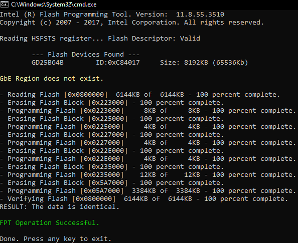
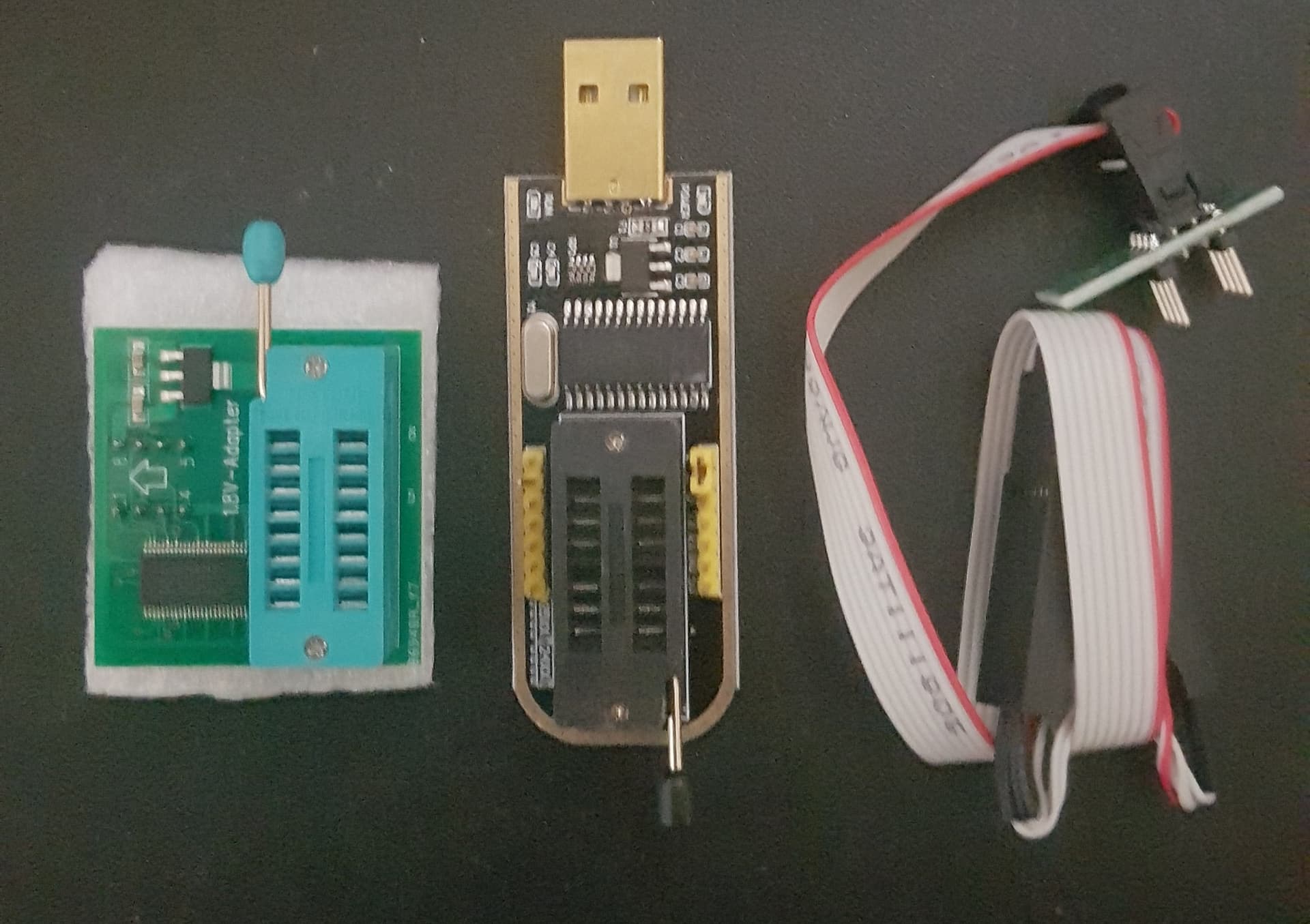
Now i have only option to flash the bios with SPI Programmer like CH341A. That’s what i think. If you guys have any suggestions beside that please share with me.

I did a lot of things but never flashed a bios with a CH341A or something else. That’s why i can’t identify the bios on the board too. First i need help to identfy the bios chip.

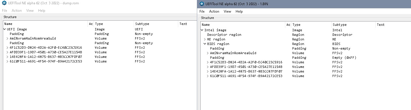
Second, i have dump file of my original bios and flashed modified bios. I can share all the files. And third how can i flash my bios?

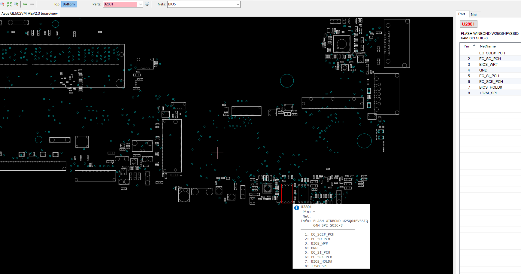
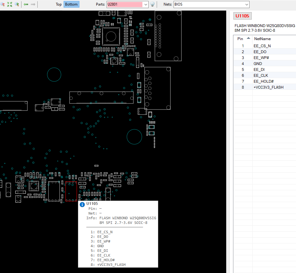
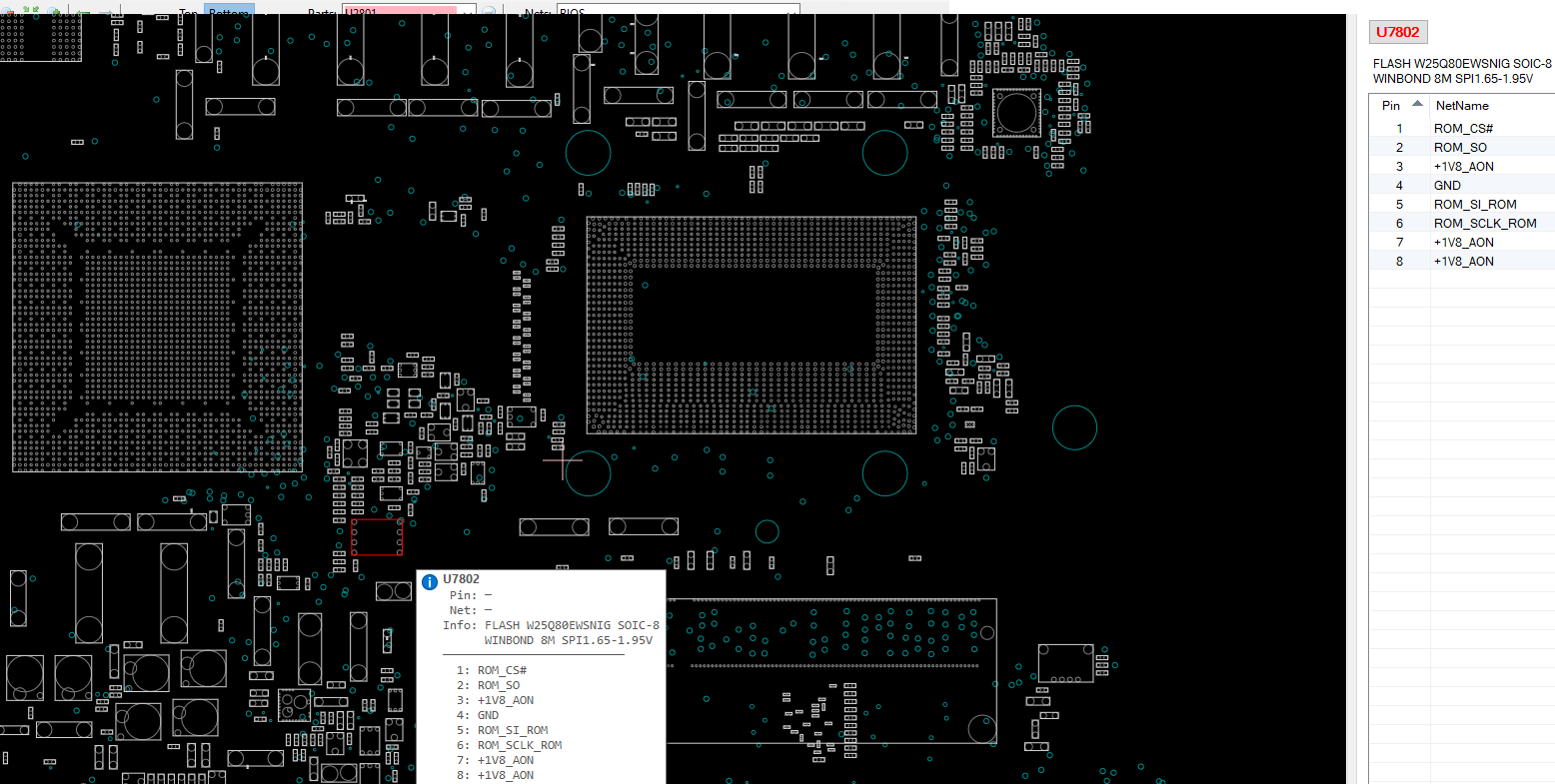
Identifying the bios chip

This is the picture of my motherboard. You can also check with the model name.

I gave numbers to the possible bios chips. I don’t know there are any chips at the back of the motherboard.

Location of 1st and 2nd chip is under the m2 ssd slot. I read 1st chip as G BH1713 / 25B64CSIG / P18437 and 2nd Winbond 25Q80DVSIG 1646

Location of 3rd chip is under the Nvidia GPU

It’s Winbond 25Q80EWNIG 1651

Do you guys have any suggestions instead of using SPI programmer? and which one is my bios chip? Is it 3 or 1,8 volts?

If you read all of this you’r a LEGEND. Thanks!

Edit by Fernando: Thread title shortened and customized

25B64CSIG might be bios, the other two chips are 2 MBit chips, seems to be a 3V chip but google the datasheet yourself.

Some machines do have an NVRAM reset procedure, can’t see it here.

CH341 Dump the content of the chip at least twice, you have to get at least two completely identical images to be sure it’s a good read.

You wrote that you have dumps of the modified and original bios- are those complete (8MB) or is it just the bios region (6MB)?

Quick search throws this up:

  1. 25B64CSIG is an 64 Mbit flash from GigaDevice, works at 3.3v.
  2. 25Q80DVSIG is an 8 Mbit flash from Winbond, 3v.
  3. 25Q80EWNIG is another 8 Mbit flash from Winbond, careful with this one as it’s one of the 1.8v (1.95 max), you’ll need an adapter to 1.8v if you use one of the cheaper CH341a based programmers.

I concur with @lfb6, #1 must be the one containing system’s firmware.

I’m afraid not, but I never had an ASUS machine and I’m not versed in reset procedures. If you’re lucky, the dump you have from before the flash and configuration is a complete one (not only the BIOS region) so it could be flashed directly, if not… I don’t know if it could be stitched into a full dump of the chip and edited so that configuration, variables, etc. are set to default values; I have yet to see how things go with AMI boards, I wouldn’t mind giving it a try, but I can’t offer no guarantee… perhaps someone else could check it.

EDIT: Some CH341a based programmers (those with a black PCB) require a modification so data lines go at 3.3v as well instead of 5v, I think Winbond chips are relatively tolerant in that department, but I thought of mentioning it just in case.

Those normally don’t need a modification (measuring from ca. 3:10) :

.
.
Please make a valid dump of the chip content before you flash anything into it. If your earlier ‘dumps’ are just bios regions you’ll need the other firmware regions to create a complete image, if your actual dump can’t be repaired (but that’s often possible).

1 Like

@JRMoore @lfb6 thank you so much for the reply guys! My original bios file from ASUS website GL502VMK-AS.308 is 6146KB (6MB) file. But i don’t know the size of my original bios dump and modded bios dump right now. I should boot my ssd from a different device (friends laptop) to get the file. I’ll try to get the dump files and whole folder and upload it soon for you guys. I live in really good area the website i am gonna buy CH341 could deliver it in 6 hours - 3 days max.

I search about this 1.8v thing. Even i never flash bios before. I think chip number 3 is a vBios or something but before i buy the CH341 device i should know which one is the bios 100%.

I got the boardview fz file of my motherboard but not sure about revision. The motherboard and all chips are same. I search for bios and it looks like 1st one is the bios. I am not sure.

If you guys check this .fz file from boardview you can see everything about the board.

Asus GL502VM REV2.0 boardview.rar (239.0 KB)

Only difference is The 1st chip is winbond at this file. But mine is Gigadevice with same ID.


I am going to 100% double back up chip content when we get into that step.

You normally need only the type of chip used on your board. Read it yourself or post a pic with readable lettering.

@lfb6 @JRMoore Ok i got the files and know what i did exactly. Even i take screenshots and picture for whole process to figure out what should i do when i fail at a step.

These are the orginal how to flash modded bios files my friend gave to me. Including my screenshots of grub environment and successfully flashed modded bios with intel flash programmer.

It contains original dump of my bios before bios modding 6144KB dump.rom and generated mod.rom modded bios file 6144KB

Also this is the original bios file provided by ASUS GL502 VMK 308 6146KB —>
GL502VMK-AS ORIGINAL BIOS.rar (4.0 MB)

These are the instructions given to me

This tool package only apply to GL502VMK with bios version 308.
Please confirm model name and bios version is the same with I modified before you do anything.

Following the step in below to generate a mod bios for your machine and flashing it.

Step1.>(dump bios from your machine)
Run dump.bat as administrator ,it will generate a bios dump that names
dump.rom , this bios file is exclusive for your machine.

Step2.>(replace modified module)
Run replace.bat as administrator ,it will replace some modified modules into step1’s dump and make a unlocked bios that names mod.rom.(It may take a while and some command windows appears.)

Step3.>(change variable of BIOS Lock)

a} Please prepare a usb flash device and format it with fat32 ,then copy folder EFI to it ,then reboot system.

b) Boot this usb device as uefi model ,it will enter to GRUB sell environment.You should now see a screen similar with grub_shell.jpg.

c) Type setup_var Setup 0x8E2 0x0 then press enter ,if no any error happen ,you will get some message about offset 0x8E2 to 0x00.

d) Type reboot to exit GRUB shell and return to operation system.

Step4.>(re-flash mod bios)

Run flash.bat as administrator to flash mod bios.
(If you still meet message “Error 368: Failed to disable write protection for the BIOS space” in fpt ,please repeat Step3 again or more times. )

Done!

I have done every step exactly and carefully. It was working without any problems when i boot to bios and windows before i disable integrated GPU accidently.

This is the picture i taken from my phone at the Step 3 - GRUB Shell.

And the screenshot i have taken at the modded bios flashing Step 4
Also it detects flash device as GD25B64B but the 1st chip (possibly bios) we talk about is 25B64CSIG. Is it detects like that because of same chip family?

Successfull Mod Flash Screen

I hope the files i provided and the screenshots i have taken going to help us. Thanks for the help guys! I can’t explain how these replies helped me mentally.

Thanks!

That are indeed just bios regions. You would need something looking like the right side:

.
NVRAM is in your case the region where settings are stored:

.
Machine specific information like serial, a/your Windows code is in the padding between NVRAM and first UEFI volume:

.
Since NVRAM doesn’t seem to contain machine specific information, it can easily emptied. Sometimes it’s possible to find the last change and to revert it, but that does rarely work. (All that given that your changes did not corrupt Thunderbolt configuration.)

1 Like

Thank you for the video!! I’ve seen quite a lot of Sorin’s repairs, but I hadn’t come across that one.

I could have swore it was one of those I was using when I burned an XMC flash chip (“burned” not in the sense that it caught fire). It was then that I learned that while Vcc was using the 3.3v regulator, the data lines were using 5v and some chips didn’t like that. I thought of me lucky, I had used that programmer in many flash chips without problems; although most were from things other than motherboards.

I don’t recall where it was, but I read about TB controllers using a smaller SPI chip near them, perhaps one of those 8 Mbit ones. My laptop is different, both in model and brand, but I also have a 28Q80DV near the Thunderbolt port.

I provide everything i can. I order CH341A programmer + SOP8 Clips + 1.8V adaptor too. :smile: Just waiting for it. As i said i never attempt to program a chip before. I learn the basics like the PIN 1 on clips, the bios chip etc. @JRMoore @lfb6 Do you guys think chip number 1 is the bios right? Then after i get the programmer what should i do? Could you guide me for that? Also, i am trying to learn so hard. What does it mean that?

Since NVRAM doesn’t seem to contain machine specific information, it can easily emptied. Sometimes it’s possible to find the last change and to revert it, but that does rarely work. (All that given that your changes did not corrupt Thunderbolt configuration.)

I can’t get anything on the screen because of disabled integrated GPU it means that if i connect thunderbolt to DP or HDMI adaptor to the port could i get the boot or bios?

The 1.8v adapter won’t be necessary, chip #1, the GigaDevice one, is the one holding the BIOS and it works at 3.3v; and it has to be that one, the other two can’t hold enough data for it.

As for guidance using a programmer sure, there ought to be several guides online in different places, using various programs, but we can tell you what to do when the time comes. In fact, the video that lfb6 posted earlier shows Sorin using one of them to read the contents of a flash chip (at around the 7 min mark), and you can also use the clip because of the package your chip is in (plainly speaking, it has legs).

You’re going to be needing another machine to do the operations of course, but after a full dump is read you could post it here. lfb6 should be able to tell you more, this is still new to me, but the idea would be to at least empty the NVRAM area in the dump before reprogramming the chip.

Okay, i get it. I want to buy the 1.8V adaptor for future applications and risks. I have a really busy schedule i don’t want to wait for another cargo. I have to do some writing, that’s why i want to fix the Bios this week. Waiting for cargo rn. @lfb6 @JRMoore Thanks a lot! And @lfb6 Still trying to understand thunderbolt thing btw :smile:

Yes, I used the black CH341 on a quite a lot of SPIs, never damaging something. And Sorins explanation seems valid.

Yes, that seems to be one way to do it. Problem isn’t the firmware (code-) part, there are settings, too. And for this mainboard the smaller SPI might be EC firmware, too, and the spi for Thunderbird might be another place (or not existing).

There’s a lot of possible configurations here. If you download the schematics for GL502VM it seems all outputs including panel are connected to the dGPU, but logically they might still be routed through iGPU and dp seems to be routed through thunderbolt.

Seems tha the 25Q80DVSIG indeed is Thunderbolt, 3rd chip 25Q80EWNIG seems to be Nvidia firmware, the latter being 1.8V!

You’ll probably find a better explanation other places, but I remember some firmwares where resetting the NVRAM settings didn’t fix the error completely

1 Like

I just wait for the programmer, thanks for the explanation. I dont think we need to program 1.8v chip but if we do it. Thats good i already order the adaptor too.

@lfb6 @JRMoore both of my cargos arrived. I have everything we need. What should i do now?

Dump/Read all the chips according the previous notes and tips, install CH341A soft and drivers, probably didnt come none with the package, correctly use the adapters on the 3,3 and 1,8v.
AC adapter off , with CMOS battery on or off, always try readings with both off for starting.

[Guide] Using CH341A-based programmer to flash SPI EEPROM - BIOS/UEFI Modding / BIOS Modding Guides and Problems - Win-Raid Forum (level1techs.com)

[GUIDE] Flash BIOS with CH341A programmer - BIOS/UEFI Modding / BIOS Modding Guides and Problems - Win-Raid Forum (level1techs.com)

[GUIDE] The Beginners Guide to Using a CH341A SPI Programmer/Flasher (With Pictures!) - BIOS/UEFI Modding / BIOS Modding Guides and Problems - Win-Raid Forum (level1techs.com)

The tricky part here is making a good connection with the clip to the SPIs and an up to date reading software with the referenced Chip IDs on the database identification of the soft.
Readings content should not present FF data on the whole reading.

DO NOT rush yourself, read and learn… you dont need a burned chip or damage motherboard.

Dump just the one bios chip, you need 2 a 100% identical dumps to be sure that you have a good read.

As MeatWar writes, positionong the clamp correctly is the worst part. I think most programs will work, I normally use ASprogrammer 1.4.

@MeatWar Thanks for the tutorials! I watched some youtube vidoes too. @lfb6 @JRMoore I successfully connected clamp and get the dumps. Before i save it, i also verify the data. I got 2 dumps from GigaDevice chip and another two dumps from Winbond 3.3V / Winbond 1.8V chip(I use the adaptor). I am not sure my clamp connection is good or not. But at least you can check the files. As i said i verified before saving it.

  • These files dumped without CMOS battery and AC Adapter.
  • I use modified version of normal CH314 Programmer software - SiberiaProg CH341A v1.45 - If it changes anything i can dump again.