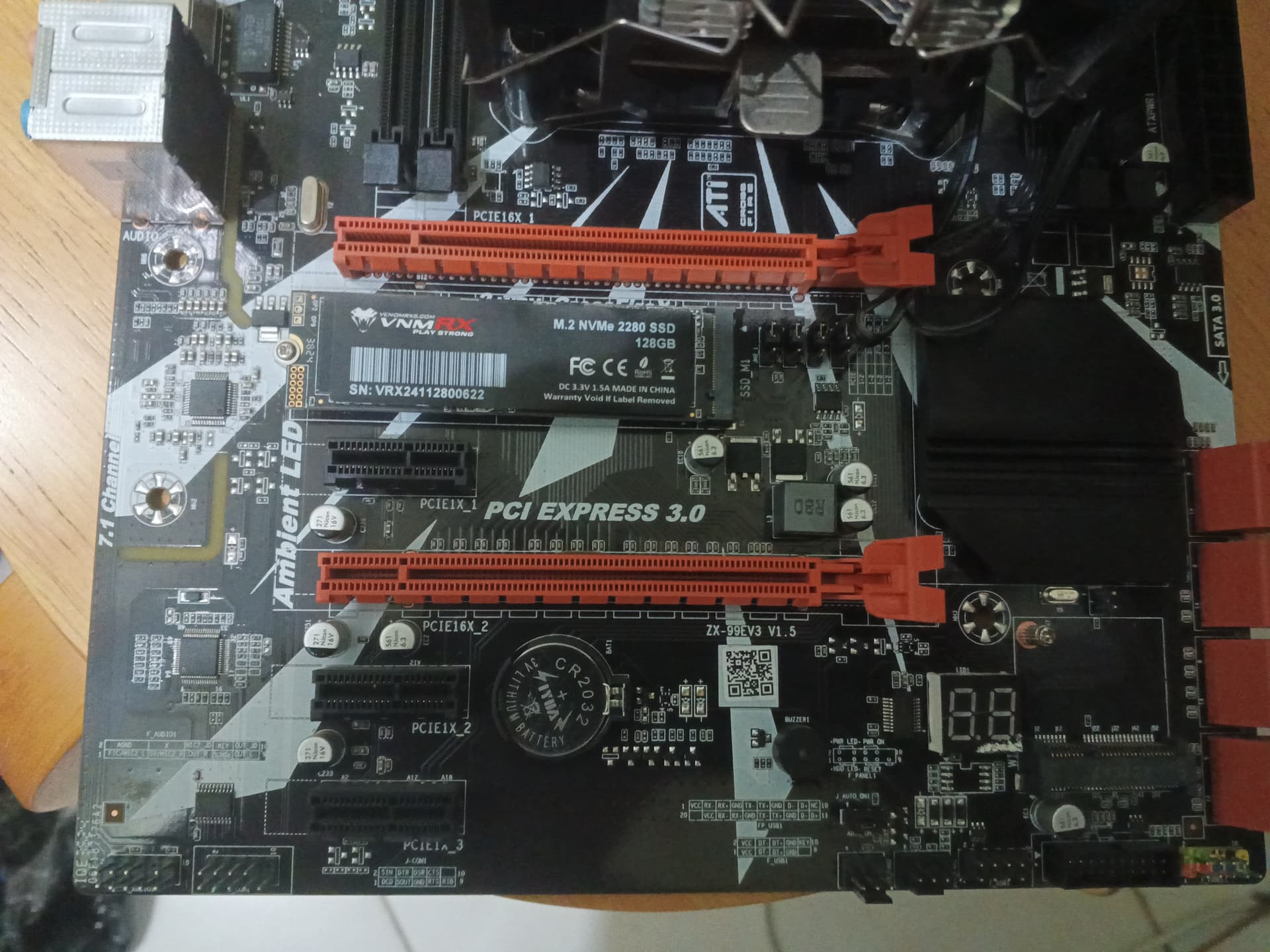
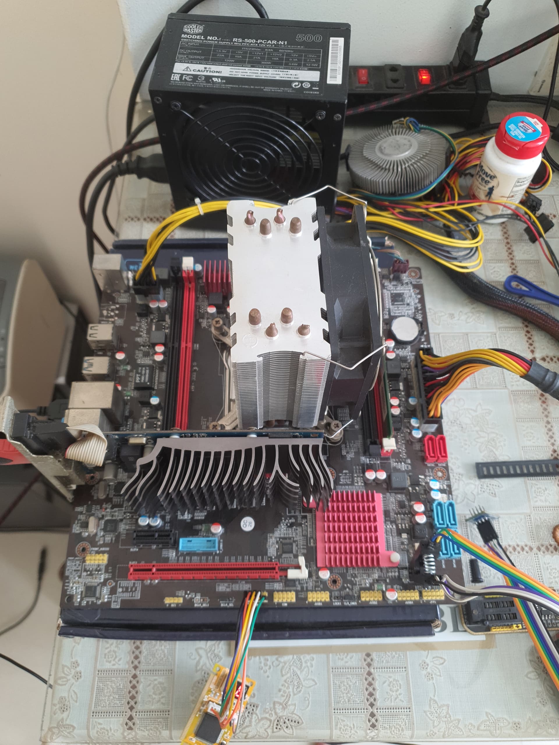
TLDR: Apart from just Windows 11, some games like Battlefield 6 are now requiring TPM to work. The key contribution of this post is establishing a general methodology on how to find out an unknown JLPC/Debug pinout, so that a TPM module can be safely and correctly connected. Nothing more than a normal digital multi-meter and around ten 2.54mm pitch female to male wires are needed. Generally speaking, the Chinese X99 boards lack any sort of official manual/documentation, and the JLPC/Debug pinout is of course no exception. General buying advice is also given, enabling a simple and solder free installation. Please understand that if you break something while attempting this, it is on you. I am also providing some information and BIOS files for two “classical” Chinese X99 motherboards
- X99Z V102, mostly sold under the Machinist or Runing brand name
- ZX-99EV3 v1.23 (also called PlexHD-X99, Atermiter X99, Kllisre X99)
Update 2026-01-03
I now have better BIOS available, see this post. Overview and old deprecated BIOS can be downloaded from here, including a simple but practical PPT template.
X99Z V102: Measuring voltages on the JLPC1 pins
- First start the computer normally, go into the BIOS and load optimal defaults, reboot, and then leave it idling in the BIOS.
- Take a multimeter, and connect the black cable to ground. I choose to use the 2 separated ground wires in a 6+2 GPU power supply cable
- Now push on a 2.54mm female on each JLPC1 pin, and then measure the voltage
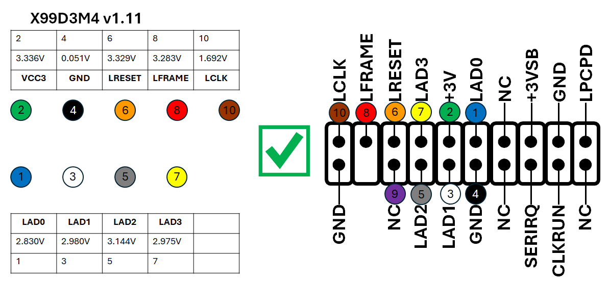
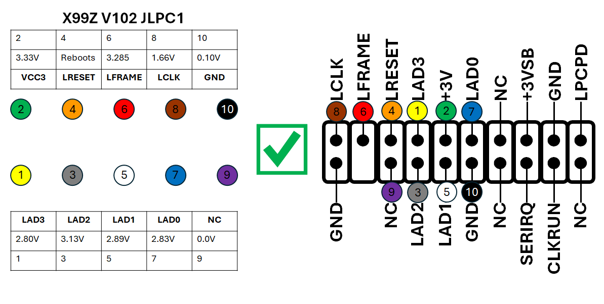
- Three pins will be very easy to determine, namely: VCC3 (3.33V), GND (~0.1V) and finally LCLK (VCC3/2~1.66V) since this is a clock signal with 50% duty cycle)
- When measuring a particular pin, I did indeed get a system reset. So I assumed that was LRESET (more on this pin later, the ZX-99EV3 behaved differently)
- I had one NC (Not Connected) pin. To be 100% sure that is was NC, I moved the black cable from power supply ground to power supply +12V. Still the multi-meter showed 0.00V.
This left me with five undetermined pins (four LADx and LFRAME). While this is on a level that can arguably be tested until it works, I still wasn’t too happy. Expressed mathematically the number of combinations are still “5!”, which equates to 120 different combinations. With that said, the most likely type of pinout is that the four data pins are next to each other (could be either 0-3 or 3-0 order). This leaves the remaining pin as LFRAME, and hence only 2 combinations to test.
After a lot of digging and reading, I happened to stumble upon the pinout for another Machinist board, and it was exactly the same on this motherboard – In a video that basically does what I set out to do (but with an extremely messy wiring method). See the specified timestamp in this video. WARNING: That video states “For any Chinese board”, but at the end of the day it just provides one common pinout. As will be shown later, the pinout for my second board was completely different. So in other words: Do not blindly trust any random diagram, you need to measure yourself to verify! Just to re-iterate, the core of this post is indeed about establishing a general methodology for finding the pinout for any motherboard, rather than just giving out the end result for one particular board.
X99Z V102: Flashing a BIOS with TPM support
It is very straight forward to get all required BIOS functionality on this board: Simply use a CH341A programmer and flash the latest official Machinist/JuXieShi X99-K9 BIOS (X9XK9 Ver:007 12/25/2023 17:07:48) on the board. Everything works perfectly. RAM timings are already unlocked by the manufacturer, and they even provide a TBU (Turbo Boost Unlocked) version if you have a Xeon 2xxxV3 series CPU. Since the download links do not work on the English version of the official page, see the first Mega link in this post. Since I am primarily gaming focused, I am also including a modified BIOS to make CPU and cache overclocking work with for instance Throttlestop. For reference, the official product page in Chinese can be found here.
X99Z V102: Selecting, wiring up, and verifying that the TPM works
The core reason why the wiring becomes terribly messy in the video I linked to before, is that the TPM female connectors are very close to each other. In technical terms, the motherboard uses a 2.54mm pitch, while the TPM module in that video uses a 2.00mm pitch. The easiest solution to all of this is simply: Check carefully and buy a TPM module that also has 2.54mm pitch, then it will be very straightforward to wire everything up. So that is what I did. When looking online on several sites, then there is typically a common/general 20-pin LPC type TPM module being sold. I checked and sure enough, it uses 2.54mm pitch. Then I bought a pack of 10cm long 2.54mm female to male cables.

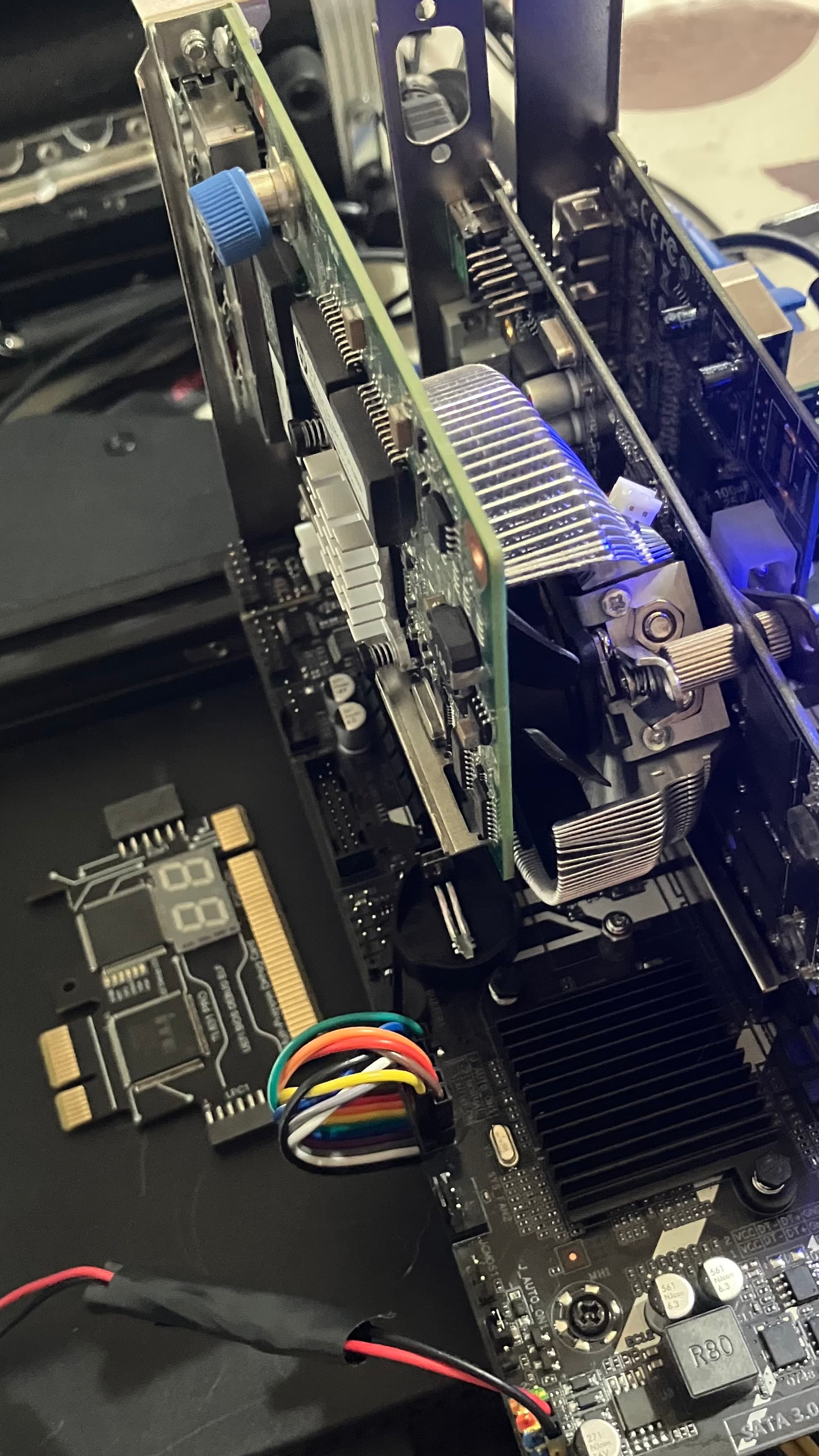
When double checking the pinout from the supplier, it didn’t make sense. From my point of view, the pinout should be what I see when I look directly at the connection header. In this case, nothing lined up. So I took this approach: I have three GND (ground) pins, that should connect to the same electrical point. So I just put the multimeter in Ohm beep testing mode and checked. The end result can be expressed as: “The manufacturer had swapped the upper and lower rows with each other”. Not rotated, swapped. So based on this, I simply re-drew the TPM module header as well, and thought one step ahead. By selecting one particular ground out of the 3 possible, I could get all 10 wires physically close to each other. This makes it easy to connect and also easy to reinforce with electrical tape. Finally I connected everything and it worked, just took a few reboots before I had something under Advanced/Trusted Computing in the BIOS. The default settings were fine, the module then shows up as avaliable in Windows.

What follows here is the core part. Since we have both measuring results and a proven pinout for the previous X99Z V102 board, we can now start comparing and see what pin is what on the unknown Debug port on the ZX-99EV3.
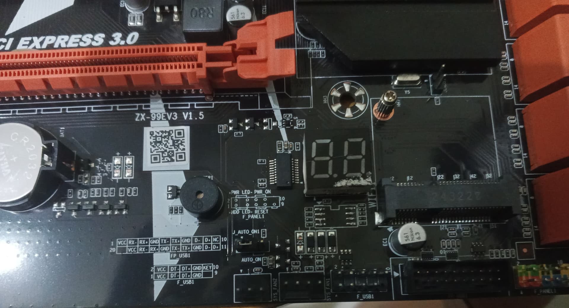
ZX-99EV3: Measuring voltage on the Debug pins
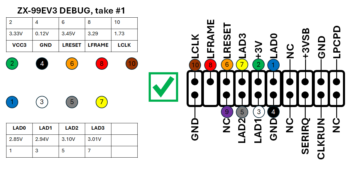
- I found VCC3, GND and LCLK very quickly just like on the first board
- I did not get a system reset when measuring. But I did find one pin which had a voltage higher than VCC3 (3.45V, ~0.12V higher than 3.33V). I made the assumption that this was reset
- Next, I assumed that the pin with a voltage just below VCC3 was still LFRAME (3.285V on the first board, 3.29V on this one)
- This left me with the 4 data pins, or at most 24 possible combinations. LAD2 had the highest voltage on the first board, so I assumed that here as well. So the first board had a 3-0 LADx order, and if I had identified LAD2 correctly, then this second board should most likely have a 0-3 LADx order.
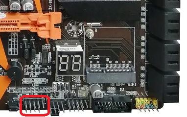
All of this qualified guessing was indeed correct, and I got the TPM up and running.
ZX-99EV3: Flashing a BIOS with TPM support
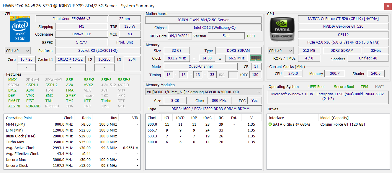
This turned out more difficult than expected, and I had to spend 1 week+ on this part alone. See the first Mega link in this post. After a lot of testing, this worked perfectly fine:
- I took the X99D4M4 complete 16M BIOS as a starting point
- I then swapped out the 8M BIOS region with the Machinist X99 MR9A PRO MAX. Yes, I know, this board does not have a C612 chipset, but typically B85. But it works perfectly
- I put in a lot of smaller changes with AMIBCP to startup with TPM and Secure Boot enabled by default, and also to enable overclocking of for instance 1660V3
- A CH341A programmer is needed to flash the BIOS